479:
lowest energy state in the conduction band and the highest energy state of the valence band of a material have the same value, then the material has a direct bandgap. If they are not the same, then the material has an indirect band gap and the electronic transition must undergo momentum transfer to satisfy conservation. Such indirect "forbidden" transitions still occur, however at very low probabilities and weaker energy. For materials with a direct band gap, valence electrons can be directly excited into the conduction band by a photon whose energy is larger than the bandgap. In contrast, for materials with an indirect band gap, a photon and
45:
533:
183:
541:
electrons across the band gap, and the rest is wasted. The semiconductors commonly used in commercial solar cells have band gaps near the peak of this curve, as it occurs in silicon-based cells. The
Shockley–Queisser limit has been exceeded experimentally by combining materials with different band gap energies to make, for example,
198:. This variation in band structure is responsible for the wide range of electrical characteristics observed in various materials. Depending on the dimension, the band structure and spectroscopy can vary. The different types of dimensions are as listed: one dimension, two dimensions, and three dimensions.
821:
binding energy, it is possible for a photon to have just barely enough energy to create an exciton (bound electron–hole pair), but not enough energy to separate the electron and hole (which are electrically attracted to each other). In this situation, there is a distinction between "optical band gap"
553:
absorbs. Strictly, a semiconductor will not absorb photons of energy less than the band gap; whereas most of the photons with energies exceeding the band gap will generate heat. Neither of them contribute to the efficiency of a solar cell. One way to circumvent this problem is based on the so-called
540:
gives the maximum possible efficiency of a single-junction solar cell under un-concentrated sunlight, as a function of the semiconductor band gap. If the band gap is too high, most daylight photons cannot be absorbed; if it is too low, then most photons have much more energy than necessary to excite
829:
In almost all inorganic semiconductors, such as silicon, gallium arsenide, etc., there is very little interaction between electrons and holes (very small exciton binding energy), and therefore the optical and electronic bandgap are essentially identical, and the distinction between them is ignored.
463:
Two-dimensional structures of solids behave because of the overlap of atomic orbitals. The simplest two-dimensional crystal contains identical atoms arranged on a square lattice. Energy splitting occurs at the
Brillouin zone edge for one-dimensional situations because of a weak periodic potential,
478:
Based on their band structure, materials are characterised with a direct band gap or indirect band gap. In the free-electron model, k is the momentum of a free electron and assumes unique values within the
Brillouin zone that outlines the periodicity of the crystal lattice. If the momentum of the
443:
It was mentioned earlier that the dimensions have different band structure and spectroscopy. For non-metallic solids, which are one dimensional, have optical properties that are dependent on the electronic transitions between valence and conduction bands. In addition, the spectroscopic transition
291:
The distinction between semiconductors and insulators is a matter of convention. One approach is to think of semiconductors as a type of insulator with a narrow band gap. Insulators with a larger band gap, usually greater than 4 eV, are not considered semiconductors and generally do not exhibit
149:
in chemistry. If the valence band is completely full and the conduction band is completely empty, then electrons cannot move within the solid because there are no available states. If the electrons are not free to move within the crystal lattice, then there is no generated current due to no net
209:
of energy, and forbidden from other regions because there are no allowable electronic states for them to occupy. The term "band gap" refers to the energy difference between the top of the valence band and the bottom of the conduction band. Electrons are able to jump from one band to another.
417:
Furthermore, lattice vibrations increase with temperature, which increases the effect of electron scattering. Additionally, the number of charge carriers within a semiconductor will increase, as more carriers have the energy required to cross the band-gap threshold and so conductivity of
464:
which produces a gap between bands. The behavior of the one-dimensional situations does not occur for two-dimensional cases because there are extra freedoms of motion. Furthermore, a bandgap can be produced with strong periodic potential for two-dimensional and three-dimensional cases.
517:
usually emit photons with energy close to and slightly larger than the band gap of the semiconductor material from which they are made. Therefore, as the band gap energy increases, the LED or laser color changes from infrared to red, through the rainbow to violet, then to UV.
229:
is a material with an intermediate-sized, non-zero band gap that behaves as an insulator at T=0K, but allows thermal excitation of electrons into its conduction band at temperatures that are below its melting point. In contrast, a material with a large band gap is an
48:
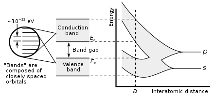
Graph of carbon atoms being brought together to form a diamond crystal, demonstrating formation of the electronic band structure and band gap. The right graph shows the energy levels as a function of the spacing between atoms. When far apart
299:
The band-gap energy of semiconductors tends to decrease with increasing temperature. When temperature increases, the amplitude of atomic vibrations increase, leading to larger interatomic spacing. The interaction between the lattice
404:
850:, band gaps or stop bands are ranges of photon frequencies where, if tunneling effects are neglected, no photons can be transmitted through a material. A material exhibiting this behaviour is known as a
822:
and "electronic band gap" (or "transport gap"). The optical bandgap is the threshold for photons to be absorbed, while the transport gap is the threshold for creating an electron–hole pair that is
77:
is such a large number, adjacent orbitals are extremely close together in energy so the orbitals can be considered a continuous energy band. At the actual diamond crystal cell size (denoted by
1483:
Feneberg, Martin; Leute, Robert A. R.; Neuschl, Benjamin; Thonke, Klaus; Bickermann, Matthias (16 August 2010). "High-excitation and high-resolution photoluminescence spectra of bulk AlN".
418:
semiconductors also increases with increasing temperature. The external pressure also influences the electronic structure of semiconductors and, therefore, their optical band gaps.
249:
is strongly dependent on the band gap. The only available charge carriers for conduction are the electrons that have enough thermal energy to be excited across the band gap and the
210:
However, in order for a valence band electron to be promoted to the conduction band, it requires a specific minimum amount of energy for the transition. This required energy is an
1523:
304:
and the free electrons and holes will also affect the band gap to a smaller extent. The relationship between band gap energy and temperature can be described by
425:
crystal, the band gap is size dependent and can be altered to produce a range of energies between the valence band and conduction band. It is also known as
1278:
150:
charge carrier mobility. However, if some electrons transfer from the valence band (mostly full) to the conduction band (mostly empty), then current
256:
Band-gap engineering is the process of controlling or altering the band gap of a material by controlling the composition of certain semiconductor
137:. It is the energy required to promote an electron from the valence band to the conduction band. The resulting conduction-band electron (and the
1335:
1125:"A thermodynamic model for determining pressure and temperature effects on the bandgap energies and other properties of some semiconductors"
155:
2016:
2001:
1760:
Xie, R.; Long, G. G.; Weigand, S. J.; Moss, S. C.; Carvalho, T.; Roorda, S.; Hejna, M.; Torquato, S.; Steinhardt, P. J. (29 July 2013).
318:
487:. Therefore, direct bandgap materials tend to have stronger light emission and absorption properties and tend to be better suited for
211:
1567:
1467:
1415:
1307:
1260:
1210:
277:
859:
563:
1957:
499:; however, indirect bandgap materials are frequently used in PVs and LEDs when the materials have other favorable properties.
1360:
238:, the valence and conduction bands may overlap, so there is no longer a bandgap with forbidden regions of electronic states.
214:
characteristic of the solid material. Electrons can gain enough energy to jump to the conduction band by absorbing either a
862:, a new class of optical disordered materials has been suggested, which support band gaps perfectly equivalent to those of
554:
photon management concept, in which case the solar spectrum is modified to match the absorption profile of the solar cell.
1376:
Dean, K J (August 1984). "Waves and Fields in
Optoelectronics: Prentice-Hall Series in Solid State Physical Electronics".
484:
1431:
Zanatta, A.R. (December 2022). "The
Shockley-Queisser limit and the conversion efficiency of silicon-based solar cells".
1762:"Hyperuniformity in amorphous silicon based on the measurement of the infinite-wavelength limit of the structure factor"
1015:
955:
473:
433:
1886:
Eichenfield, Matt; Chan, Jasper; Camacho, Ryan M.; Vahala, Kerry J.; Painter, Oskar (2009). "Optomechanical crystals".
537:
174:
either have very small band gaps or none, because the valence and conduction bands overlap to form a continuous band.
85:
limits the number of electrons in a single orbital to two, and the bands are filled beginning with the lowest energy.
562:
Below are band gap values for some selected materials. For a comprehensive list of band gaps in semiconductors, see
2006:
1033:
891:
426:
261:
1680:"Unraveling exciton dynamics in amorphous silicon dioxide: Interpretation of the optical features from 8 to 11 eV"
1594:"Revisiting the optical bandgap of semiconductors and the proposal of a unified methodology to its determination"
945:
437:
269:
206:
195:
187:
114:
82:
31:
1058:
1996:
1976:
950:
858:
has broadened the range of photonic band gap materials, beyond photonic crystals. By applying the technique in
1275:
970:
901:
265:
246:
242:
159:
483:
must both be involved in a transition from the valence band top to the conduction band bottom, involving a
81:), two bands are formed, called the valence and conduction bands, separated by a 5.5 eV band gap. The
44:
831:
572:
273:
163:
141:
in the valence band) are free to move within the crystal lattice and serve as charge carriers to conduct
2011:
960:
130:
94:
272:. It is also possible to construct layered materials with alternating compositions by techniques like
1905:
1842:
1773:
1734:
1691:
1652:
1492:
1173:
1136:
1010:
975:
508:
492:
235:
231:
171:
37:
This article is about the electronic bandgap found in semiconductors. For the photonic band gap, see
1000:
90:
421:
In a regular semiconductor crystal, the band gap is fixed owing to continuous energy states. In a
1937:
1895:
1832:
1707:
1929:
1921:
1868:
1801:
1625:
1563:
1463:
1411:
1356:
1331:
1303:
1256:
1216:
1206:
926:
693:
601:
542:
293:
1679:
30:
This article is about solid state physics. For voltage control circuitry in electronics, see
1913:
1858:
1850:
1791:
1781:
1742:
1699:
1660:
1615:
1605:
1500:
1440:
1385:
1181:
1164:
Varshni, Y.P. (January 1967). "Temperature dependence of the energy gap in semiconductors".
1144:
1043:
911:
878:
851:
754:
711:
142:
110:
38:
532:
162:
of a solid. Substances having large band gaps (also called "wide" band gaps) are generally
1282:
916:
906:
855:
835:
792:
772:
729:
675:
182:
126:
1909:
1846:
1777:
1738:
1695:
1656:
1496:
1177:
1140:
1863:
1820:
1796:
1761:
1620:
1593:
1518:
444:
probability is between the initial and final orbital and it depends on the integral. φ
1990:
1711:
1559:
1389:
1185:
1149:
1124:
1063:
1005:
990:
985:
965:
896:
584:
550:
488:
309:
305:
250:
226:
167:
138:
134:
1964:
1941:
1038:
1020:
867:
122:
118:
1643:
Bauer, J. (1977). "Optical properties, band gap, and surface roughness of Si3N4".
549:
The optical band gap (see below) determines what portion of the solar spectrum a
1972:
940:
514:
496:
422:
281:
1703:
1610:
1504:
826:
bound together. The optical bandgap is at lower energy than the transport gap.
1555:
1444:
995:
980:
527:
285:
1925:
1786:
1746:
1664:
1220:
1053:
1048:
921:
847:
657:
146:
117:
of solids, the band gap refers to the energy difference (often expressed in
1933:
1872:
1805:
1629:
1819:
Yu, Sunkyu; Piao, Xianji; Hong, Jiho; Park, Namkyoo (16 September 2015).
1200:
202:
1917:
65:, their electron orbitals begin to spatially overlap and hybridize into
1854:
863:
818:
639:
619:
460:
is the integral, ε is the electric vector, and u is the dipole moment.
296:
also plays a role in determining a material's informal classification.
17:
874:
624:
588:
480:
301:
219:
215:
1837:
1821:"Bloch-like waves in random-walk potentials based on supersymmetry"
1900:
531:
399:{\displaystyle E_{g}(T)=E_{g}(0)-{\frac {\alpha T^{2}}{T+\beta }}}
257:
181:
166:, those with small band gaps (also called "narrow" band gaps) are
43:
1725:
Baumeister, P.W. (1961). "Optical
Absorption of Cuprous Oxide".
158:). Therefore, the band gap is a major factor determining the
61:
with the same energies. However, when the atoms come closer
1678:
Vella, E.; Messina, F.; Cannas, M.; Boscaino, R. (2011).
69:
molecular orbitals each with a different energy, where
1458:
Tropf, W.J.; Harris, T.J.; Thomas, M.E. (2000). "11".
27:
Energy range in a solid where no electron states exist
321:
292:
semiconductive behaviour under practical conditions.
398:
253:that are left off when such an excitation occurs.
1965:"Energy Gap (and what makes glass transparent?)"
1406:Goetzberger, A.; Knobloch, J.; Voss, B. (1998).
1293:
1291:
1202:The electronic structure and chemistry of solids
1095:The Electronic Structure and Chemistry of Solids
1766:Proceedings of the National Academy of Sciences
1110:Solid State Devices and Technology, 3rd Edition
276:. These methods are exploited in the design of
1401:
1399:
73:is the number of atoms in the crystal. Since
53:all the atoms have discrete valence orbitals
8:
1545:
1543:
1541:
1539:
1537:
1535:
1587:
1585:
1583:
1581:
1579:
1550:Streetman, Ben G.; Sanjay Banerjee (2000).
1298:Yu, P.Y.; Cardona, M. (1996). "Chapter 6".
1285:. Evidenttech.com. Retrieved on 2013-04-03.
568:
1899:
1862:
1836:
1795:
1785:
1619:
1609:
1246:
1244:
1242:
1240:
1238:
1236:
1234:
1232:
1230:
1148:
376:
366:
348:
326:
320:
109:, is an energy range in a solid where no
1074:
194:Every solid has its own characteristic
1251:Pankove, J.I. (1971). "Chapters 1-3".
838:, the distinction may be significant.
503:Light-emitting diodes and laser diodes
1321:
1319:
308:'s empirical expression (named after
7:
1351:Sze, S.M. (1981). "Chapters 12–14".
1205:. Oxford : Oxford University Press.
1088:
1086:
1084:
1082:
1080:
1078:
830:However, in some systems, including
413:(0), α and β are material constants.
156:carrier generation and recombination
1524:Introduction to Solid State Physics
1253:Optical processes in semiconductors
842:Band gaps for other quasi-particles
278:heterojunction bipolar transistors
201:In semiconductors and insulators,
25:
1958:Direct Band Gap Energy Calculator
813:Optical versus electronic bandgap
1353:Physics of semiconductor devices
1326:Fox, M. (2008). "Chapters 1–3".
860:supersymmetric quantum mechanics
145:. It is closely related to the
1408:Crystalline silicon solar cells
564:List of semiconductor materials
1552:Solid State electronic Devices
1300:Fundamentals of semiconductors
1123:Ünlü, Hilmi (September 1992).
836:single-walled carbon nanotubes
360:
354:
338:
332:
1:
1592:Zanatta, A.R. (August 2019).
1328:Optical properties of solids
1186:10.1016/0031-8914(67)90062-6
1150:10.1016/0038-1101(92)90170-H
1016:Strongly correlated material
956:Direct and indirect bandgaps
474:Direct and indirect bandgaps
468:Direct and indirect band gap
205:are confined to a number of
1034:Wide-bandgap semiconductors
873:Similar physics applies to
2033:
2017:Nuclear magnetic resonance
2002:Electronic band structures
1704:10.1103/PhysRevB.83.174201
1611:10.1038/s41598-019-47670-y
1505:10.1103/PhysRevB.82.075208
1390:10.1088/0031-9112/35/8/023
934:List of electronics topics
892:Aluminium gallium arsenide
817:In materials with a large
525:
506:
471:
427:quantum confinement effect
36:
29:
1445:10.1016/j.rio.2022.100320
1410:. John Wiley & Sons.
1355:. John Wiley & Sons.
946:Bandgap voltage reference
452:is the final orbital, ʃ φ
448:is the initial orbital, φ
438:electronic band structure
121:) between the top of the
115:electronic band structure
83:Pauli exclusion principle
32:Bandgap voltage reference
1977:University of Nottingham
1108:Babu, V. Suresh (2010).
951:Condensed matter physics
432:Band gaps can be either
247:intrinsic semiconductors
178:In semiconductor physics
113:exist. In graphs of the
1787:10.1073/pnas.1220106110
1747:10.1103/PhysRev.121.359
1665:10.1002/pssa.2210390205
1645:Physica Status Solidi A
1460:Electro-Optics Handbook
1129:Solid-State Electronics
971:Field-effect transistor
902:Indium gallium arsenide
538:Shockley–Queisser limit
160:electrical conductivity
1330:. Oxford Univ. Press.
1276:“Evident Technologies”
832:organic semiconductors
546:
400:
274:molecular-beam epitaxy
191:
125:and the bottom of the
86:
1825:Nature Communications
1011:Semiconductor devices
961:Electrical conduction
535:
493:light-emitting diodes
401:
196:energy-band structure
185:
95:solid-state chemistry
51:(right side of graph)
47:
1059:Moss–Burstein effect
976:Light-emitting diode
509:Light-emitting diode
319:
1918:10.1038/nature08524
1910:2009Natur.462...78E
1847:2015NatCo...6.8269Y
1778:2013PNAS..11013250X
1772:(33): 13250–13254.
1739:1961PhRv..121..359B
1696:2011PhRvB..83q4201V
1657:1977PSSAR..39..411B
1497:2010PhRvB..82g5208F
1199:Cox, P. A. (1987).
1178:1967Phy....34..149V
1141:1992SSEle..35.1343U
1097:. pp. 102–114.
1001:Solid state physics
436:, depending on the
91:solid-state physics
1963:Moriarty, Philip.
1855:10.1038/ncomms9269
1598:Scientific Reports
1281:2009-02-06 at the
1093:Cox, P.A. (1987).
547:
543:tandem solar cells
522:Photovoltaic cells
434:direct or indirect
396:
192:
87:
2007:Quantum mechanics
1684:Physical Review B
1485:Physical Review B
1337:978-0-19-850613-3
927:Metallic hydrogen
854:. The concept of
810:
809:
694:Gallium phosphide
602:Aluminium nitride
558:List of band gaps
551:photovoltaic cell
440:of the material.
394:
294:Electron mobility
111:electronic states
16:(Redirected from
2024:
1980:
1946:
1945:
1903:
1883:
1877:
1876:
1866:
1840:
1816:
1810:
1809:
1799:
1789:
1757:
1751:
1750:
1722:
1716:
1715:
1675:
1669:
1668:
1640:
1634:
1633:
1623:
1613:
1589:
1574:
1573:
1554:(5th ed.).
1547:
1530:
1529:
1515:
1509:
1508:
1480:
1474:
1473:
1455:
1449:
1448:
1428:
1422:
1421:
1403:
1394:
1393:
1378:Physics Bulletin
1373:
1367:
1366:
1348:
1342:
1341:
1323:
1314:
1313:
1295:
1286:
1273:
1267:
1266:
1248:
1225:
1224:
1196:
1190:
1189:
1161:
1155:
1154:
1152:
1135:(9): 1343–1352.
1120:
1114:
1113:
1105:
1099:
1098:
1090:
1044:Spectral density
912:Gallium arsenide
879:phononic crystal
852:photonic crystal
755:Lead(II) sulfide
712:Gallium arsenide
569:
405:
403:
402:
397:
395:
393:
382:
381:
380:
367:
353:
352:
331:
330:
143:electric current
101:, also called a
39:Photonic crystal
21:
2032:
2031:
2027:
2026:
2025:
2023:
2022:
2021:
1997:Electron states
1987:
1986:
1984:
1962:
1954:
1949:
1894:(7269): 78–82.
1885:
1884:
1880:
1818:
1817:
1813:
1759:
1758:
1754:
1727:Physical Review
1724:
1723:
1719:
1677:
1676:
1672:
1642:
1641:
1637:
1591:
1590:
1577:
1570:
1562:. p. 524.
1549:
1548:
1533:
1519:Kittel, Charles
1517:
1516:
1512:
1482:
1481:
1477:
1470:
1462:. McGraw-Hill.
1457:
1456:
1452:
1430:
1429:
1425:
1418:
1405:
1404:
1397:
1375:
1374:
1370:
1363:
1350:
1349:
1345:
1338:
1325:
1324:
1317:
1310:
1297:
1296:
1289:
1283:Wayback Machine
1274:
1270:
1263:
1250:
1249:
1228:
1213:
1198:
1197:
1193:
1163:
1162:
1158:
1122:
1121:
1117:
1107:
1106:
1102:
1092:
1091:
1076:
1072:
1030:
1025:
936:
931:
917:Gallium nitride
907:Indium arsenide
887:
856:hyperuniformity
844:
815:
800:
793:Copper(I) oxide
780:
773:Silicon dioxide
741:
737:
730:Silicon nitride
676:Gallium nitride
560:
530:
524:
511:
505:
485:momentum change
476:
470:
459:
455:
451:
447:
411:
383:
372:
368:
344:
322:
317:
316:
180:
127:conduction band
42:
35:
28:
23:
22:
15:
12:
11:
5:
2030:
2028:
2020:
2019:
2014:
2009:
2004:
1999:
1989:
1988:
1982:
1981:
1960:
1953:
1952:External links
1950:
1948:
1947:
1878:
1811:
1752:
1717:
1690:(17): 174201.
1670:
1651:(2): 411–418.
1635:
1604:: 11225–12pp.
1575:
1568:
1531:
1510:
1475:
1468:
1450:
1439:: 100320–7pp.
1423:
1416:
1395:
1368:
1361:
1343:
1336:
1315:
1308:
1287:
1268:
1261:
1226:
1211:
1191:
1172:(1): 149–154.
1156:
1115:
1100:
1073:
1071:
1068:
1067:
1066:
1061:
1056:
1051:
1046:
1041:
1036:
1029:
1026:
1024:
1023:
1018:
1013:
1008:
1003:
998:
993:
988:
983:
978:
973:
968:
963:
958:
953:
948:
943:
937:
935:
932:
930:
929:
924:
919:
914:
909:
904:
899:
894:
888:
886:
883:
843:
840:
814:
811:
808:
807:
805:
802:
798:
795:
790:
787:
786:
784:
781:
778:
775:
770:
766:
765:
763:
760:
757:
752:
748:
747:
745:
742:
739:
735:
732:
727:
723:
722:
720:
717:
714:
709:
705:
704:
702:
699:
696:
691:
687:
686:
684:
681:
678:
673:
669:
668:
666:
663:
660:
655:
651:
650:
648:
645:
642:
637:
633:
632:
630:
627:
622:
617:
613:
612:
610:
607:
604:
599:
595:
594:
591:
581:
578:
575:
559:
556:
526:Main article:
523:
520:
507:Main article:
504:
501:
472:Main article:
469:
466:
457:
453:
449:
445:
415:
414:
409:
392:
389:
386:
379:
375:
371:
365:
362:
359:
356:
351:
347:
343:
340:
337:
334:
329:
325:
251:electron holes
188:band structure
186:Semiconductor
179:
176:
135:semiconductors
26:
24:
14:
13:
10:
9:
6:
4:
3:
2:
2029:
2018:
2015:
2013:
2010:
2008:
2005:
2003:
2000:
1998:
1995:
1994:
1992:
1985:
1978:
1974:
1970:
1969:Sixty Symbols
1966:
1961:
1959:
1956:
1955:
1951:
1943:
1939:
1935:
1931:
1927:
1923:
1919:
1915:
1911:
1907:
1902:
1897:
1893:
1889:
1882:
1879:
1874:
1870:
1865:
1860:
1856:
1852:
1848:
1844:
1839:
1834:
1830:
1826:
1822:
1815:
1812:
1807:
1803:
1798:
1793:
1788:
1783:
1779:
1775:
1771:
1767:
1763:
1756:
1753:
1748:
1744:
1740:
1736:
1732:
1728:
1721:
1718:
1713:
1709:
1705:
1701:
1697:
1693:
1689:
1685:
1681:
1674:
1671:
1666:
1662:
1658:
1654:
1650:
1646:
1639:
1636:
1631:
1627:
1622:
1617:
1612:
1607:
1603:
1599:
1595:
1588:
1586:
1584:
1582:
1580:
1576:
1571:
1569:0-13-025538-6
1565:
1561:
1560:Prentice Hall
1557:
1553:
1546:
1544:
1542:
1540:
1538:
1536:
1532:
1527:
1526:, 7th Edition
1525:
1520:
1514:
1511:
1506:
1502:
1498:
1494:
1491:(7): 075208.
1490:
1486:
1479:
1476:
1471:
1469:9780070687165
1465:
1461:
1454:
1451:
1446:
1442:
1438:
1434:
1427:
1424:
1419:
1417:0-471-97144-8
1413:
1409:
1402:
1400:
1396:
1391:
1387:
1383:
1379:
1372:
1369:
1364:
1358:
1354:
1347:
1344:
1339:
1333:
1329:
1322:
1320:
1316:
1311:
1309:3-540-61461-3
1305:
1301:
1294:
1292:
1288:
1284:
1280:
1277:
1272:
1269:
1264:
1262:0-486-60275-3
1258:
1254:
1247:
1245:
1243:
1241:
1239:
1237:
1235:
1233:
1231:
1227:
1222:
1218:
1214:
1212:0-19-855204-1
1208:
1204:
1203:
1195:
1192:
1187:
1183:
1179:
1175:
1171:
1167:
1160:
1157:
1151:
1146:
1142:
1138:
1134:
1130:
1126:
1119:
1116:
1111:
1104:
1101:
1096:
1089:
1087:
1085:
1083:
1081:
1079:
1075:
1069:
1065:
1064:Urbach energy
1062:
1060:
1057:
1055:
1052:
1050:
1047:
1045:
1042:
1040:
1037:
1035:
1032:
1031:
1027:
1022:
1019:
1017:
1014:
1012:
1009:
1007:
1006:Semiconductor
1004:
1002:
999:
997:
994:
992:
991:Photovoltaics
989:
987:
986:Photoresistor
984:
982:
979:
977:
974:
972:
969:
967:
966:Electron hole
964:
962:
959:
957:
954:
952:
949:
947:
944:
942:
939:
938:
933:
928:
925:
923:
920:
918:
915:
913:
910:
908:
905:
903:
900:
898:
897:Boron nitride
895:
893:
890:
889:
884:
882:
880:
876:
871:
869:
868:quasicrystals
865:
861:
857:
853:
849:
841:
839:
837:
833:
827:
825:
820:
812:
806:
803:
796:
794:
791:
789:
788:
785:
782:
776:
774:
771:
768:
767:
764:
761:
758:
756:
753:
750:
749:
746:
743:
733:
731:
728:
725:
724:
721:
718:
715:
713:
710:
707:
706:
703:
700:
697:
695:
692:
689:
688:
685:
682:
679:
677:
674:
671:
670:
667:
664:
661:
659:
656:
653:
652:
649:
646:
643:
641:
638:
635:
634:
631:
628:
626:
623:
621:
618:
615:
614:
611:
608:
605:
603:
600:
597:
596:
592:
590:
586:
582:
579:
576:
574:
571:
570:
567:
565:
557:
555:
552:
544:
539:
534:
529:
521:
519:
516:
510:
502:
500:
498:
494:
490:
489:photovoltaics
486:
482:
475:
467:
465:
461:
441:
439:
435:
430:
428:
424:
419:
412:
390:
387:
384:
377:
373:
369:
363:
357:
349:
345:
341:
335:
327:
323:
315:
314:
313:
311:
310:Y. P. Varshni
307:
303:
297:
295:
289:
287:
283:
279:
275:
271:
267:
263:
259:
254:
252:
248:
244:
239:
237:
233:
228:
227:semiconductor
223:
221:
217:
213:
208:
204:
199:
197:
189:
184:
177:
175:
173:
169:
168:semiconductor
165:
161:
157:
153:
148:
147:HOMO/LUMO gap
144:
140:
139:electron hole
136:
132:
128:
124:
120:
119:electronvolts
116:
112:
108:
104:
100:
96:
92:
84:
80:
76:
72:
68:
64:
60:
56:
52:
46:
40:
33:
19:
2012:Spectroscopy
1983:
1968:
1891:
1887:
1881:
1828:
1824:
1814:
1769:
1765:
1755:
1730:
1726:
1720:
1687:
1683:
1673:
1648:
1644:
1638:
1601:
1597:
1551:
1522:
1513:
1488:
1484:
1478:
1459:
1453:
1436:
1432:
1426:
1407:
1381:
1377:
1371:
1352:
1346:
1327:
1302:. Springer.
1299:
1271:
1252:
1201:
1194:
1169:
1165:
1159:
1132:
1128:
1118:
1109:
1103:
1094:
1039:Band bending
1021:Valence band
872:
845:
828:
823:
816:
561:
548:
515:laser diodes
512:
497:laser diodes
495:(LEDs), and
477:
462:
442:
431:
420:
416:
407:
298:
290:
282:laser diodes
255:
243:conductivity
240:
224:
218:(heat) or a
200:
193:
151:
123:valence band
106:
102:
98:
88:
78:
74:
70:
66:
62:
58:
54:
50:
1973:Brady Haran
1831:(1): 8269.
1433:Results Opt
941:Electronics
423:quantum dot
286:solar cells
63:(left side)
1991:Categories
1838:1501.02591
1733:(2): 359.
1556:New Jersey
1384:(8): 339.
1362:0471056618
1070:References
996:Solar cell
981:Photodiode
593:Reference
583:Band gap (
528:Solar cell
260:, such as
236:conductors
172:conductors
164:insulators
154:flow (see
131:insulators
107:energy gap
1926:0028-0836
1901:0906.1236
1712:121793038
1255:. Dover.
1112:. Peason.
1054:Tauc plot
1049:Pseudogap
922:Germanium
885:Materials
848:photonics
658:Germanium
513:LEDs and
391:β
370:α
364:−
232:insulator
222:(light).
212:intrinsic
203:electrons
1975:for the
1934:19838165
1873:26373616
1806:23898166
1630:31375719
1528:. Wiley.
1279:Archived
1221:14213060
1028:See also
864:crystals
577:Material
406:, where
280:(HBTs),
99:band gap
1942:4404647
1906:Bibcode
1864:4595658
1843:Bibcode
1797:3746861
1774:Bibcode
1735:Bibcode
1692:Bibcode
1653:Bibcode
1621:6677798
1493:Bibcode
1174:Bibcode
1166:Physica
1137:Bibcode
875:phonons
819:exciton
640:Silicon
620:Diamond
587:) @ 302
491:(PVs),
306:Varshni
302:phonons
103:bandgap
18:Bandgap
1940:
1932:
1924:
1888:Nature
1871:
1861:
1804:
1794:
1710:
1628:
1618:
1566:
1466:
1414:
1359:
1334:
1306:
1259:
1219:
1209:
769:IV–VI
751:IV–VI
708:III–V
690:III–V
672:III–V
598:III–V
580:Symbol
481:phonon
270:InAlAs
268:, and
266:InGaAs
262:GaAlAs
258:alloys
220:photon
216:phonon
170:, and
1938:S2CID
1896:arXiv
1833:arXiv
1708:S2CID
877:in a
762:0.37
726:IV–V
719:1.43
716:GaAs
701:2.26
665:0.67
647:1.14
573:Group
234:. In
207:bands
1930:PMID
1922:ISSN
1869:PMID
1802:PMID
1626:PMID
1564:ISBN
1464:ISBN
1412:ISBN
1357:ISBN
1332:ISBN
1304:ISBN
1257:ISBN
1217:OCLC
1207:ISBN
834:and
804:2.1
759:PbS
698:GaP
683:3.4
680:GaN
629:5.5
609:6.0
606:AlN
536:The
284:and
241:The
133:and
97:, a
93:and
57:and
1914:doi
1892:462
1859:PMC
1851:doi
1792:PMC
1782:doi
1770:110
1743:doi
1731:121
1700:doi
1661:doi
1616:PMC
1606:doi
1501:doi
1441:doi
1386:doi
1182:doi
1145:doi
866:or
846:In
824:not
777:SiO
662:Ge
654:IV
644:Si
636:IV
616:IV
456:ûεφ
312:),
245:of
152:can
129:in
105:or
89:In
1993::
1971:.
1967:.
1936:.
1928:.
1920:.
1912:.
1904:.
1890:.
1867:.
1857:.
1849:.
1841:.
1827:.
1823:.
1800:.
1790:.
1780:.
1768:.
1764:.
1741:.
1729:.
1706:.
1698:.
1688:83
1686:.
1682:.
1659:.
1649:39
1647:.
1624:.
1614:.
1600:.
1596:.
1578:^
1558::
1534:^
1521:.
1499:.
1489:82
1487:.
1435:.
1398:^
1382:35
1380:.
1318:^
1290:^
1229:^
1215:.
1180:.
1170:34
1168:.
1143:.
1133:35
1131:.
1127:.
1077:^
881:.
870:.
801:O
797:Cu
783:9
744:5
734:Si
585:eV
566:.
429:.
288:.
264:,
225:A
1979:.
1944:.
1916::
1908::
1898::
1875:.
1853::
1845::
1835::
1829:6
1808:.
1784::
1776::
1749:.
1745::
1737::
1714:.
1702::
1694::
1667:.
1663::
1655::
1632:.
1608::
1602:9
1572:.
1507:.
1503::
1495::
1472:.
1447:.
1443::
1437:9
1420:.
1392:.
1388::
1365:.
1340:.
1312:.
1265:.
1223:.
1188:.
1184::
1176::
1153:.
1147::
1139::
799:2
779:2
740:4
738:N
736:3
625:C
589:K
545:.
458:i
454:f
450:f
446:i
410:g
408:E
388:+
385:T
378:2
374:T
361:)
358:0
355:(
350:g
346:E
342:=
339:)
336:T
333:(
328:g
324:E
190:.
79:a
75:N
71:N
67:N
59:s
55:p
41:.
34:.
20:)
Text is available under the Creative Commons Attribution-ShareAlike License. Additional terms may apply.