702:(Small Outline IC), a surface-mount package which is currently very popular, particularly in consumer electronics and personal computers, is essentially a shrunk version of the standard IC PDIP, the fundamental difference which makes it an SMT device being a second bend in the leads to flatten them parallel to the bottom plane of the plastic housing. The SOJ (Small Outline J-lead) and other SMT packages with "SOP" (for "Small Outline Package") in their names can be considered further relatives of the DIP, their original ancestor. SOIC packages tend to have half the pitch of DIP, and SOP are half that, a fourth of DIP. (0.1"/2.54 mm, 0.05"/1.27 mm, and 0.025"/0.635 mm, respectively)
439:(barely visible to the naked human eye) are welded between these die periphery contacts and bond pads on the die itself, connecting one lead to each bond pad, and making the final connection between the microcircuits and the external DIP leads. The bond wires are not usually taut but loop upward slightly to allow slack for thermal expansion and contraction of the materials; if a single bond wire breaks or detaches, the entire IC may become useless. The top of the package covers all of this delicate assemblage without crushing the bond wires, protecting it from contamination by foreign materials.
60:
336:
355:
367:
49:
219:
324:
312:
668:
38:
255:(SOIC), though DIPs continued in extensive use through the 1990s, and still continue to be used substantially as the year 2011 passes. Because some modern chips are available only in surface-mount package types, a number of companies sell various prototyping adapters to allow those surface-mount devices (SMD) to be used like DIP devices with through-hole breadboards and soldered prototyping boards (such as
390:
163:
398:
414:, the SMT package that most resembles a typical DIP, appears essentially the same, notwithstanding size scale, except that after being bent down the leads are bent upward again by an equal angle to become parallel with the bottom plane of the package.) In ceramic (CERDIP) packages, an epoxy or grout is used to hermetically seal the two halves together, providing an
462:(around the contained electronic components) with a hard translucent epoxy material from which the leads emerge. Others, such as DIP switches, are composed of two (or more) plastic housing parts snapped, welded, or glued together around a set of contacts and tiny mechanical parts, with the leads emerging through molded-in holes or notches in the plastic.
547:
1018:
149:, possibly including a heat sink tab in place of the second row of pins, and types with four rows of pins, two rows, staggered, on each side of the package. DIP packages have been mostly displaced by surface-mount package types, which avoid the expense of drilling holes in a PCB and which allow higher density of interconnections.
586:
447:
number of leads which a practical DIP package may have. Even for a very small die with many bond pads (e.g. a chip with 15 inverters, requiring 32 leads), a wider DIP would still be required to accommodate the radiating leads internally. This is one of the reasons that four-sided and multiple rowed packages, such as
434:
Inside the package, the lower half has the leads embedded, and at the center of the package is a rectangular space, chamber, or void into which the IC die is cemented. The leads of the package extend diagonally inside the package from their positions of emergence along the periphery to points along a
461:
Some other types of DIP devices are built very differently. Most of these have molded plastic housings and straight leads or leads that extend directly out of the bottom of the package. For some, LED displays particularly, the housing is usually a hollow plastic box with the bottom/back open, filled
137:
that supports the device die and provides connection pins. Some types of IC are made in ceramic DIP packages, where high temperature or high reliability is required, or where the device has an optical window to the interior of the package. Most DIP packages are secured to a PCB by inserting the pins
226:
The original dual-in-line package was invented by Bryant "Buck" Rogers in 1964 while working for
Fairchild Semiconductor. The first devices had 14 pins and looked much like they do today. The rectangular shape allowed integrated circuits to be packaged more densely than previous round packages. The
405:
The body (housing) of a DIP containing an IC chip is usually made from molded plastic or ceramic. The hermetic nature of a ceramic housing is preferred for extremely high reliability devices. However, the vast majority of DIPs are manufactured via a thermoset molding process in which an epoxy mold
607:, has the same dimensions as a DIL package, but the leads on each side are bent into an alternating zigzag configuration so as to fit four lines of solder pads (instead of two with a DIL). The QIL design increased the spacing between solder pads without increasing package size, for two reasons:
446:
The necessity of laying out all of the leads in a basically radial pattern in a single plane from the die perimeter to two rows on the periphery of the package is the main reason that DIP packages with higher lead counts must have wider spacing between the lead rows, and it effectively limits the
129:
is the total number of pins, and sometimes appended with the row-to-row package width "N" for narrow (0.3") or "W" for wide (0.6"). For example, a microcircuit package with two rows of seven vertical leads would be a DIP14 or DIP14N. The photograph at the upper right shows three DIP14 ICs. Common
442:
Usually, a company logo, alphanumeric codes and sometimes words are printed on top of the package to identify its manufacturer and type, when it was made (usually as a year and a week number), sometimes where it was made, and other proprietary information (perhaps revision numbers, manufacturing
639:
standards use an inter-lead spacing (lead pitch) of 0.1 inches (2.54 mm) (JEDEC MS-001BA). Row spacing varies depending on lead counts, with 0.3 in. (7.62 mm) (JEDEC MS-001) or 0.6 inch (15.24 mm) (JEDEC MS-011) the most common. Less common standardized row spacings include
430:
is not achieved because the plastic itself is usually somewhat porous to moisture and the process cannot ensure a good microscopic seal between the leads and the plastic at all points around the perimeter. However, contaminants are usually still kept out well enough that the device can operate
293:
or in sockets. Sockets allow easy replacement of a device and eliminates the risk of damage from overheating during soldering. Generally sockets were used for high-value or large ICs, which cost much more than the socket. Where devices would be frequently inserted and removed, such as in test
509:) wide DIP, normally when clarification is needed e.g. for DIP with 24 pins or more, which usually come in "wide" 0.600 in wide DIP package. An example of a typical proper full spec for a "narrow" DIP package would be 300 mil body width, 0.1 inches (2.54 mm) pin pitch.
130:
packages have as few as three and as many as 64 leads. Many analog and digital integrated circuit types are available in DIP packages, as are arrays of transistors, switches, light emitting diodes, and resistors. DIP plugs for ribbon cables can be used with standard IC sockets.
409:
The leads emerge from the longer sides of the package along the seam, parallel to the top and bottom planes of the package, and are bent downward approximately 90 degrees (or slightly less, leaving them angled slightly outward from the centerline of the package body). (The
708:(PGA) packages may be considered to have evolved from the DIP. PGAs with the same 0.1 inches (2.54 mm) pin centers as most DIPs were popular for microprocessors from the early to mid-1980s through the 1990s. Owners of personal computers containing Intel
675:
As shown in the diagram, leads are numbered consecutively from Pin 1. When the identifying notch in the package is at the top, Pin 1 is the top left corner of the device. Sometimes Pin 1 is identified with an indent or paint dot mark.
651:(NC) leads to the internal chip, or are duplicated, e.g. two ground pins. For 0.6 inch spacing, typical lead counts are 24, 28, 32, and 40; less common are 36, 42, 48, 52, and 64 lead counts. Some microprocessors, such as the
138:
through holes in the board and soldering them in place. Where replacement of the parts is necessary, such as in test fixtures or where programmable devices must be removed for changes, a DIP socket is used. Some sockets include a
471:
1022:
689:
In addition to providing for human visual identification of the orientation of the package, the notch allows automated chip-insertion machinery to confirm correct orientation of the chip by mechanical sensing.
646:
The number of leads is always even. For 0.3 inch spacing, typical lead counts are 8, 14, 16, 18, and 28; less common are 4, 6, 20, and 24 lead counts. To have an even number of leads some DIPs have unused
231:
machine and passed on to automated testing machines, with very little human labor required. DIP packages were still large with respect to the integrated circuits within them. By the end of the 20th century,
640:
0.4 inch (10.16 mm) (JEDEC MS-010) and 0.9 inch (22.86 mm), as well as a row spacing of 0.3 inch, 0.6 inch or 0.75 inch with a 0.07 inch (1.778 mm) lead pitch.
274:, DIPs remained popular for many years due to their easy handling with external programming circuitry (i.e., the DIP devices could be simply plugged into a socket on the programming device.) However, with
335:
263:). (SMT can pose quite a problem, at least an inconvenience, for prototyping in general; most of the characteristics of SMT that are advantages for mass production are difficulties for prototyping.)
354:
301:
DIPs are also used with breadboards, a temporary mounting arrangement for education, design development or device testing. Some hobbyists, for one-off construction or permanent prototyping, use
227:
package was well-suited to automated assembly equipment; a PCB could be populated with scores or hundreds of ICs, then all the components on the circuit board could be soldered at one time on a
281:
Through the 1990s, devices with fewer than 20 leads were manufactured in a DIP format in addition to the newer formats. Since about 2000, newer devices are often unavailable in the DIP format.
406:
compound is heated and transferred under pressure to encapsulate the device. Typical cure cycles for the resins are less than 2 minutes and a single cycle may produce hundreds of devices.
210:
blocks on to which discrete components could be soldered were used where groups of components needed to be easily removed, for configuration changes, optional features or calibration.
679:
For example, for a 14-lead DIP, with the notch at the top, the left leads are numbered from 1 to 7 (top to bottom) and the right row of leads are numbered 8 to 14 (bottom to top).
524:(OTP) versions. Windowed and windowless packages were also used for microcontrollers, and other devices, containing EPROM memory. Windowed CERDIP-packaged EPROMs were used for the
570:
chips and multiple resistors with a common pin. As compared to DIPs with a typical maximum pin count of 64, SIPs have a typical maximum pin count of 24 with lower package costs.
531:
Molded plastic DIPs are much lower in cost than ceramic packages; one 1979 study showed that a plastic 14 pin DIP cost around US$ 0.063 and a ceramic package cost US$ 0.82.
366:
243:
DIPs were the mainstream of the microelectronics industry in the 1970s and 1980s. Their use has declined in the first decade of the 21st century due to the emerging new
1113:
643:
The former Soviet Union and
Eastern bloc countries used similar packages, but with a metric pin-to-pin spacing of 2.5 mm rather than 0.1 inches (2.54 mm).
311:
751:
323:
1567:
111:); eventually microprocessors and similar complex devices required more leads than could be put on a DIP package, leading to development of higher-density
1508:
1086:
979:
305:
wiring with DIPs, and their appearance when physically inverted as part of this method inspires the informal term "dead bug style" for the method.
31:
528:
ROM of many early IBM PC clones with an adhesive label covering the window to prevent inadvertent erasure through exposure to ambient light.
1420:
1106:
426:
inside. Plastic DIP (PDIP) packages are usually sealed by fusing or cementing the plastic halves around the leads, but a high degree of
103:
R&D in 1964, when the restricted number of leads available on circular transistor-style packages became a limitation in the use of
1477:
1357:
1062:
1001:
944:
901:
880:
860:
727:. The similarity is such that a PGA socket may be physically compatible with some DIP devices, though the converse is rarely true.
516:
were sold in ceramic DIPs manufactured with a circular window of clear quartz over the chip die to allow the part to be erased by
1347:
1342:
699:
411:
252:
821:
1560:
1099:
1033:
686:, relays, or devices that replace leads with a heat sink fin). The remaining leads are numbered as if all positions had leads.
236:
packages allowed further reduction in the size and weight of systems. DIP chips are still popular for circuit prototyping on a
41:
1027:
59:
1151:
458:
CPU) has long leads inside the package between pins and the die, making such a package unsuitable for high speed devices.
1503:
615:. This may seem odd today, given the far closer solder pad spacing in use now, but in the 1970s, the heyday of the QIL,
1599:
1386:
302:
248:
1534:
It is relatively common to find packages that contain other components than their designated ones, such as diodes or
115:. Furthermore, square and rectangular packages made it easier to route printed-circuit traces beneath the packages.
1553:
1391:
1352:
1337:
1322:
574:
170:
incorporating four DIP ICs, a DIP LED bargraph display (upper left), and a DIP 7-segment LED display (lower left)
133:
DIP packages are usually made from an opaque molded epoxy plastic pressed around a tin-, silver-, or gold-plated
965:
99:(PCB) or inserted in a socket. The dual-inline format was invented by Don Forbes, Rex Rice and Bryant Rogers at
1518:
1182:
772:
423:
244:
233:
222:
Breadboard prototype: Ultrasonic microphone preamp build with SMD-parts soldered to DIP and SIP breakout boards
435:
rectangular perimeter surrounding the die, tapering as they go to become fine contacts at the die. Ultra-fine
1523:
1362:
777:
290:
100:
92:
1691:
1332:
1306:
912:
746:
713:
1513:
1482:
1122:
506:
275:
96:
88:
1696:
1498:
1381:
1174:
720:
626:
track between 2 solder pads. This was very handy on the then standard single sided single layer PCBs.
598:
376:
360:
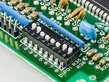
0.3" wide DIP socket for narrow DIP28 IC, also known as DIP28N, commonly used on older
Arduino boards
341:
295:
183:
146:
139:
278:(ISP) technology now state of the art, this advantage of DIPs is rapidly losing importance as well.
1440:
1163:
659:, used lead counts as high as 64; this is typically the maximum number of leads for a DIP package.
566:) has one row of connecting pins. It is not as popular as the DIP, but has been used for packaging
271:
91:
with a rectangular housing and two parallel rows of electrical connecting pins. The package may be
55:
ICs in 0.6" wide ceramic DIP40W, DIP32W, DIP28W, DIP24W packages, also known as CDIP (Ceramic DIP)
1467:
1457:
175:
104:
1617:
573:
One variant of the single in-line package uses part of the lead frame for a heat sink tab. This
520:. Often, the same chips were also sold in less expensive windowless PDIP or CERDIP packages as
218:
1535:
1396:
1068:
1058:
997:
940:
897:
876:
856:
517:
196:
DIP connector plugs for ribbon cables are common in computers and other electronic equipment.
186:
48:
44:
logic ICs in 0.3" wide 14-pin plastic DIP packages (DIP14N), also known as PDIP (Plastic DIP)
1289:
1283:
1277:
1265:
1253:
1247:
1235:
1139:
107:. Increasingly complex circuits required more signal and power supply leads (as observed in
72:
1472:
1425:
1415:
797:
716:
683:
200:
719:
processors may be most familiar with these PGA packages, which were often inserted into
203:(RTC) modules which contained an IC chip and a non-replaceable 10-year lithium battery.
1660:
1609:
1430:
762:
705:
667:
652:
455:
448:
228:
108:
37:
1685:
828:
648:
616:
1586:
1037:
800:" in the context of switches. Another phrase used is D.N.C. (for "Do not connect").
736:
145:
Variations of the DIP package include those with only a single row of pins, e.g. a
112:
796:
The abbreviation N.C. (for "Not connected" or "No connect") is also used to mean "
162:
724:
540:
482:
Several DIP variants for ICs exist, mostly distinguished by packaging material:
474:
Several PDIPs and CERDIPs. The large CERDIP in the foreground is an NEC 8080AF (
427:
389:
499:– A denser version of the PDIP with a 0.07 in (1.778 mm) lead pitch.
1577:
741:
656:
546:
475:
256:
237:
207:
179:
167:
134:
64:
1072:
317:
0.3" wide DIP sockets with dual-wipe contacts for 16-, 14-, and 8-pin DIP ICs
1462:
612:
436:
260:
397:
980:
Integrated circuit, hybrid, and multichip module package design guidelines
1670:
1654:
1649:
1643:
1637:
1632:
1627:
1622:
1091:
756:
419:
577:
is useful for such applications as audio power amplifiers, for example.
431:
reliably for decades with reasonable care in a controlled environment.
372:
17:
1271:
1259:
1241:
1229:
1157:
1145:
957:
924:
623:
329:
0.3" wide 16-pin DIP socket with machined round contacts for DIP16 IC
1545:
470:
401:
Dual in-line (DIP) integrated circuit metal tape base with contacts
1223:
1217:
1211:
1205:
1131:
709:
666:
636:
584:
545:
521:
513:
469:
396:
388:
345:
267:
217:
190:
161:
58:
52:
47:
36:
1199:
1193:
1187:
590:
585:
525:
505:– Sometimes used to refer to a "narrow" 0.300 in. (or 300
178:(ICs). Other devices in DIP packages include resistor networks,
1549:
1095:
619:
of neighbouring solder pads on DIL chips was an issue at times,
767:
567:
550:
Package sample for single in-line package (SIP or SIL) devices
415:
937:
Microelectronics
Packaging Handbook: Semiconductor packaging
935:
Rao R. Tummala, Eugene J. Rymaszewski, Alan G. Klopfenstein
240:
because of how easily they can be inserted and used there.
344:(ZIF) socket for 0.6" wide DIP28W IC, commonly used on
1665:
non-Intel modification of the original Intel Socket 7
454:
A large DIP package (such as the DIP64 used for the
1608:
1584:
1491:
1439:
1408:
1371:
1315:
1299:
1173:
1129:
30:"PDIP" redirects here. The term may also refer to
199:Dallas Semiconductor manufactured integrated DIP
622:QIL also increased the possibility of running a
166:An operating prototyped circuit on a solderless
189:and bar graph displays, and electromechanical
1561:
1107:
1087:DIP packages documentation, photos and videos
752:List of integrated circuit package dimensions
487:Ceramic dual in-line package (CERDIP or CDIP)
8:
682:Leads are skipped on some DIP devices (e.g.
635:Commonly found DIP packages that conform to
451:, were introduced (around the early 1980s).
393:Side view of a dual in-line package (DIP) IC
503:Skinny dual in-line package (SDIP or SPDIP)
497:Shrink plastic dual in-line package (SPDIP)
1568:
1554:
1546:
1509:List of integrated circuit packaging types
1114:
1100:
1092:
996:(3rd ed.). McGraw-Hill. p. 42.
759:(a larger 19-pin DIP, introduced in 1967)
379:8-bit microcontroller in DIP28N IC socket
992:Kang, Sung-Mo; Leblebici, Yusuf (2002).
913:Computer Museum retrieved April 16, 2008
871:Jackson, Kenneth.A.; Schröter, Wolfgang
67:with 0.3" wide 16-pin (DIP16N) footprint
1166:(SOD-123 / SOD-323 / SOD-523 / SOD-923)
813:
789:
307:
32:Indonesian Democratic Party of Struggle
968:from the original on August 18, 2021.
894:Electronic Inventions and Discoveries
853:Electronic Inventions and Discoveries
7:
873:Handbook of Semiconductor Technology
443:plant codes, or stepping ID codes.)
27:Type of electronic component package
492:Plastic dual in-line package (PDIP)
925:http://www.microchip.com/packaging
671:Pin numbering is counter-clockwise
294:equipment or EPROM programmers, a
118:A DIP is usually referred to as a
25:
1021: This article incorporates
1016:
994:CMOS digital integrated circuits
365:
353:
334:
322:
310:
253:small-outline integrated circuit
1034:General Services Administration
593:-based microcontroller in a QIP
1148:(DO-7 / DO-26 / DO-35 / DO-41)
958:"Single-in-Line Package (SIP)"
875:, John Wiley & Sons, 2000
663:Orientation and lead numbering
289:DIPs can be mounted either by
266:For programmable devices like
1:
422:tight seal to protect the IC
1538:in transistor packages, etc.
1504:Integrated circuit packaging
603:The QIP, sometimes called a
478:-compatible) microprocessor.
89:electronic component package
855:(2nd ed)., Pergamon Press,
249:plastic leaded chip carrier
174:DIPs are commonly used for
1713:
596:
575:multi-leaded power package
538:
29:
1532:
923:For instance, Microchip:
611:It allowed more reliable
1519:Surface-mount technology
773:Surface-mount technology
539:Not to be confused with
245:surface-mount technology
1524:Through-hole technology
896:2nd ed. Pergamon Press
778:Zig-zag in-line package
247:(SMT) packages such as
1154:(MELF / SOD-80 / LL34)
1123:Semiconductor packages
1029:Federal Standard 1037C
1023:public domain material
747:Flatpack (electronics)
684:segmented LED displays
672:
631:Lead count and spacing
594:
556:single in-line package
551:
479:
402:
394:
298:socket would be used.
291:through-hole soldering
223:
171:
68:
56:
45:
1514:Printed circuit board
670:
588:
549:
522:one-time programmable
473:
400:
392:
276:In-System Programming
221:
165:
97:printed circuit board
62:
51:
40:
1499:Electronic packaging
599:Quad in-line package
342:Zero insertion force
296:zero insertion force
140:zero insertion force
93:through-hole mounted
77:dual in-line package
176:integrated circuits
105:integrated circuits
1536:voltage regulators
1055:Packaging Databook
978:Pecht, M. (1994).
822:"see for instance"
673:
595:
552:
480:
403:
395:
375:UNO R2 board with
224:
172:
69:
57:
46:
1679:
1678:
1543:
1542:
1292:(Super-247) (SMT)
1286:(Super-220) (SMT)
1160:(SMA / SMB / SMC)
939:, Springer, 1997
518:ultraviolet light
142:(ZIF) mechanism.
16:(Redirected from
1704:
1570:
1563:
1556:
1547:
1116:
1109:
1102:
1093:
1076:
1042:
1041:
1036:. Archived from
1020:
1019:
1008:
1007:
989:
983:
976:
970:
969:
954:
948:
933:
927:
921:
915:
910:
904:
890:
884:
869:
863:
849:
843:
842:
840:
839:
833:
827:. Archived from
826:
818:
801:
794:
369:
357:
338:
326:
314:
158:Types of devices
73:microelectronics
21:
1712:
1711:
1707:
1706:
1705:
1703:
1702:
1701:
1682:
1681:
1680:
1675:
1604:
1580:
1574:
1544:
1539:
1528:
1487:
1435:
1404:
1367:
1311:
1295:
1169:
1125:
1120:
1083:
1065:
1057:. Mcgraw-Hill.
1052:
1049:
1047:Further reading
1026:
1017:
1015:
1012:
1011:
1004:
991:
990:
986:
977:
973:
956:
955:
951:
934:
930:
922:
918:
911:
907:
892:Dummer, G.W.A.
891:
887:
870:
866:
851:Dummer, G.W.A.
850:
846:
837:
835:
831:
824:
820:
819:
815:
810:
805:
804:
798:Normally closed
795:
791:
786:
733:
696:
665:
633:
601:
583:
544:
537:
468:
387:
380:
370:
361:
358:
349:
339:
330:
327:
318:
315:
287:
216:
201:real-time clock
160:
155:
35:
28:
23:
22:
15:
12:
11:
5:
1710:
1708:
1700:
1699:
1694:
1684:
1683:
1677:
1676:
1674:
1673:
1668:
1661:Super Socket 7
1658:
1652:
1647:
1641:
1635:
1630:
1625:
1620:
1614:
1612:
1606:
1605:
1603:
1602:
1597:
1591:
1589:
1582:
1581:
1575:
1573:
1572:
1565:
1558:
1550:
1541:
1540:
1533:
1530:
1529:
1527:
1526:
1521:
1516:
1511:
1506:
1501:
1495:
1493:
1492:Related topics
1489:
1488:
1486:
1485:
1480:
1475:
1470:
1465:
1460:
1455:
1452:
1449:
1445:
1443:
1437:
1436:
1434:
1433:
1428:
1423:
1418:
1412:
1410:
1406:
1405:
1403:
1402:
1399:
1394:
1389:
1384:
1379:
1375:
1373:
1369:
1368:
1366:
1365:
1360:
1358:TSSOP / HTSSOP
1355:
1350:
1345:
1340:
1335:
1330:
1325:
1319:
1317:
1313:
1312:
1310:
1309:
1303:
1301:
1297:
1296:
1294:
1293:
1287:
1281:
1275:
1269:
1263:
1257:
1251:
1245:
1239:
1233:
1227:
1221:
1215:
1209:
1203:
1197:
1191:
1185:
1179:
1177:
1171:
1170:
1168:
1167:
1161:
1155:
1149:
1143:
1136:
1134:
1127:
1126:
1121:
1119:
1118:
1111:
1104:
1096:
1090:
1089:
1082:
1081:External links
1079:
1078:
1077:
1063:
1053:Intel (1996).
1048:
1045:
1044:
1043:
1040:on 2022-01-22.
1010:
1009:
1002:
984:
971:
949:
928:
916:
905:
885:
864:
844:
812:
811:
809:
806:
803:
802:
788:
787:
785:
782:
781:
780:
775:
770:
765:
763:Pin grid array
760:
754:
749:
744:
739:
732:
729:
706:Pin grid array
695:
692:
664:
661:
653:Motorola 68000
632:
629:
628:
627:
620:
597:Main article:
582:
579:
536:
535:Single in-line
533:
511:
510:
500:
494:
489:
467:
464:
456:Motorola 68000
386:
383:
382:
381:
371:
364:
362:
359:
352:
350:
348:IC programmers
340:
333:
331:
328:
321:
319:
316:
309:
303:point-to-point
286:
283:
229:wave soldering
215:
212:
159:
156:
154:
151:
147:resistor array
63:Eight-contact
26:
24:
14:
13:
10:
9:
6:
4:
3:
2:
1709:
1698:
1695:
1693:
1692:Chip carriers
1690:
1689:
1687:
1672:
1669:
1666:
1662:
1659:
1656:
1653:
1651:
1648:
1645:
1642:
1639:
1636:
1634:
1631:
1629:
1626:
1624:
1621:
1619:
1616:
1615:
1613:
1611:
1607:
1601:
1598:
1596:
1593:
1592:
1590:
1588:
1583:
1579:
1571:
1566:
1564:
1559:
1557:
1552:
1551:
1548:
1537:
1531:
1525:
1522:
1520:
1517:
1515:
1512:
1510:
1507:
1505:
1502:
1500:
1497:
1496:
1494:
1490:
1484:
1481:
1479:
1476:
1474:
1471:
1469:
1466:
1464:
1461:
1459:
1456:
1453:
1450:
1447:
1446:
1444:
1442:
1438:
1432:
1429:
1427:
1424:
1422:
1419:
1417:
1414:
1413:
1411:
1407:
1400:
1398:
1395:
1393:
1390:
1388:
1385:
1383:
1380:
1377:
1376:
1374:
1370:
1364:
1361:
1359:
1356:
1354:
1351:
1349:
1346:
1344:
1341:
1339:
1336:
1334:
1331:
1329:
1326:
1324:
1321:
1320:
1318:
1314:
1308:
1305:
1304:
1302:
1298:
1291:
1288:
1285:
1282:
1280:(D3PAK) (SMT)
1279:
1276:
1274:(D2PAK) (SMT)
1273:
1270:
1268:(I2PAK) (SMT)
1267:
1264:
1261:
1258:
1255:
1252:
1249:
1246:
1243:
1240:
1237:
1234:
1231:
1228:
1225:
1222:
1219:
1216:
1213:
1210:
1207:
1204:
1201:
1198:
1195:
1192:
1189:
1186:
1184:
1181:
1180:
1178:
1176:
1172:
1165:
1162:
1159:
1156:
1153:
1150:
1147:
1144:
1141:
1138:
1137:
1135:
1133:
1128:
1124:
1117:
1112:
1110:
1105:
1103:
1098:
1097:
1094:
1088:
1085:
1084:
1080:
1074:
1070:
1066:
1064:1-55512-254-X
1060:
1056:
1051:
1050:
1046:
1039:
1035:
1031:
1030:
1024:
1014:
1013:
1005:
1003:0-07-246053-9
999:
995:
988:
985:
982:. Wiley-IEEE.
981:
975:
972:
967:
963:
959:
953:
950:
946:
945:0-412-08441-4
942:
938:
932:
929:
926:
920:
917:
914:
909:
906:
903:
902:0-08-022730-9
899:
895:
889:
886:
882:
881:3-527-29835-5
878:
874:
868:
865:
862:
861:0-08-022730-9
858:
854:
848:
845:
834:on 2020-09-30
830:
823:
817:
814:
807:
799:
793:
790:
783:
779:
776:
774:
771:
769:
766:
764:
761:
758:
755:
753:
750:
748:
745:
743:
740:
738:
735:
734:
730:
728:
726:
722:
718:
715:
711:
707:
703:
701:
693:
691:
687:
685:
680:
677:
669:
662:
660:
658:
654:
650:
649:not connected
644:
641:
638:
630:
625:
621:
618:
614:
610:
609:
608:
606:
600:
592:
587:
580:
578:
576:
571:
569:
565:
561:
557:
548:
542:
534:
532:
529:
527:
523:
519:
515:
508:
504:
501:
498:
495:
493:
490:
488:
485:
484:
483:
477:
472:
465:
463:
459:
457:
452:
450:
444:
440:
438:
432:
429:
425:
421:
417:
413:
407:
399:
391:
384:
378:
374:
368:
363:
356:
351:
347:
343:
337:
332:
325:
320:
313:
308:
306:
304:
299:
297:
292:
284:
282:
279:
277:
273:
269:
264:
262:
258:
254:
250:
246:
241:
239:
235:
234:surface-mount
230:
220:
213:
211:
209:
204:
202:
197:
194:
192:
188:
185:
181:
177:
169:
164:
157:
152:
150:
148:
143:
141:
136:
131:
128:
124:
123:
116:
114:
113:chip carriers
110:
106:
102:
98:
94:
90:
86:
82:
78:
74:
66:
61:
54:
50:
43:
39:
33:
19:
1664:
1663:(1996–1999;
1594:
1483:WL-CSP / WLP
1353:TSOP / HTSOP
1327:
1262:(DPAK) (SMT)
1256:(IPAK) (SMT)
1250:(TH / Panel)
1244:(TH / Panel)
1238:(TH / Panel)
1232:(TH / Panel)
1220:(TH / Panel)
1190:(TH / Panel)
1054:
1038:the original
1028:
993:
987:
974:
961:
952:
936:
931:
919:
908:
893:
888:
872:
867:
852:
847:
836:. Retrieved
829:the original
816:
792:
737:Chip carrier
725:motherboards
704:
697:
688:
681:
678:
674:
645:
642:
634:
604:
602:
581:Quad in-line
572:
563:
559:
555:
553:
530:
512:
502:
496:
491:
486:
481:
460:
453:
445:
441:
433:
408:
404:
385:Construction
300:
288:
280:
265:
242:
225:
205:
198:
195:
180:DIP switches
173:
153:Applications
144:
132:
126:
121:
119:
117:
84:
80:
76:
70:
1697:CPU sockets
1657:(1995–1997)
1646:(1994–1995)
1578:CPU sockets
1401:QUIP / QUIL
723:sockets on
694:Descendants
605:QIL package
589:A Rockwell
564:SIL package
541:SIPP memory
428:hermeticity
251:(PLCC) and
109:Rent's rule
42:4000-series
1686:Categories
1618:486 Socket
1409:Grid array
1348:SOP / SSOP
1300:Single row
1183:SOT / TSOT
838:2010-01-02
808:References
742:DIP switch
657:Zilog Z180
476:Intel 8080
437:bond wires
377:ATmega328P
257:stripboard
238:breadboard
168:breadboard
135:lead frame
65:DIP switch
1463:Flip Chip
1382:QIP / QIL
1343:SO / SOIC
1333:Flat Pack
1328:DIP / DIL
1307:SIP / SIL
1175:3...5-pin
1073:906673879
883:page 610
613:soldering
261:perfboard
187:segmented
101:Fairchild
1671:Socket 8
1655:Socket 7
1650:Socket 6
1644:Socket 5
1638:Socket 4
1633:Socket 3
1628:Socket 2
1623:Socket 1
1587:packages
1372:Quad row
1316:Dual row
966:Archived
947:page 395
757:NORBIT 2
731:See also
712:through
617:bridging
466:Variants
420:moisture
285:Mounting
125:, where
87:) is an
1142:(DO-27)
1130:Single
962:EE Semi
717:Pentium
373:Arduino
1640:(1993)
1585:Other
1576:Early
1290:TO-274
1284:TO-273
1278:TO-268
1272:TO-263
1266:TO-262
1260:TO-252
1254:TO-251
1248:TO-247
1242:TO-220
1236:TO-202
1230:TO-126
1158:DO-214
1152:DO-213
1146:DO-204
1140:DO-201
1071:
1061:
1000:
943:
900:
879:
859:
624:copper
514:EPROMs
268:EPROMs
208:header
191:relays
18:CERDIP
1441:Wafer
1224:TO-92
1218:TO-66
1212:TO-39
1206:TO-18
1132:diode
1025:from
832:(PDF)
825:(PDF)
784:Notes
710:80286
637:JEDEC
346:EPROM
95:to a
53:EPROM
1610:PGAs
1600:PLCC
1478:UICC
1421:eWLB
1387:PLCC
1338:MSOP
1226:(TH)
1214:(TH)
1208:(TH)
1202:(TH)
1200:TO-8
1196:(TH)
1194:TO-5
1188:TO-3
1069:OCLC
1059:ISBN
998:ISBN
941:ISBN
898:ISBN
877:ISBN
857:ISBN
700:SOIC
698:The
655:and
591:6502
526:BIOS
449:PGAs
418:and
412:SOIC
272:GALs
270:and
259:and
214:Uses
206:DIP
75:, a
1595:DIP
1468:PoP
1458:CSP
1454:COG
1451:COF
1448:COB
1431:PGA
1426:LGA
1416:BGA
1397:QFP
1392:QFN
1378:LCC
1363:ZIP
1323:DFN
1164:SOD
768:QFP
721:ZIF
568:RAM
562:or
560:SIP
507:mil
424:die
416:air
184:LED
120:DIP
85:DIL
83:or
81:DIP
71:In
1688::
1473:QP
1067:.
1032:.
964:.
960:.
714:P5
554:A
193:.
182:,
1667:)
1569:e
1562:t
1555:v
1115:e
1108:t
1101:v
1075:.
1006:.
841:.
558:(
543:.
127:n
122:n
79:(
34:.
20:)
Text is available under the Creative Commons Attribution-ShareAlike License. Additional terms may apply.