1035:
301:
technology tops out at a clock rate around 200 MHz (400 MT/s). Higher performance DDR chips exist, but JEDEC has stated that they will not be standardized. These chips are mostly standard DDR chips that have been tested and rated to be capable of operation at higher clock rates by the manufacturer. Such chips draw significantly more power than slower-clocked chips, but usually offered little or no improvement in real-world performance. DDR2 started to become competitive against the older DDR standard by the end of 2004, as modules with lower latencies became available.
1070:
331:
323:
315:
50:
339:
received or transmitted its data over the data bus in two data bus clock cycles (each clock cycle transferred two bits of data). Increasing the prefetch length allowed DDR2 SDRAM to double the rate at which data could be transferred over the data bus without a corresponding doubling in the rate at which the DRAM array could be accessed. DDR2 SDRAM was designed with such a scheme to avoid an excessive increase in power consumption.
281:. Alternatively, DDR2 memory operating at twice the external data bus clock rate as DDR may provide twice the bandwidth with the same latency. The best-rated DDR2 memory modules are at least twice as fast as the best-rated DDR memory modules. The maximum capacity on commercially available DDR2 DIMMs is 8GB, but chipset support and availability for those DIMMs is sparse and more common 2GB per DIMM are used.
1030:
DDR2-xxx denotes data transfer rate, and describes raw DDR chips, whereas PC2-xxxx denotes theoretical bandwidth (with the last two digits truncated), and is used to describe assembled DIMMs. Bandwidth is calculated by taking transfers per second and multiplying by eight. This is because DDR2 memory
300:
DDR2 was officially introduced in the second quarter of 2003 at two initial clock rates: 200 MHz (referred to as PC2-3200) and 266 MHz (PC2-4200). Both performed worse than the original DDR specification due to higher latency, which made total access times longer. However, the original DDR
1180:
was commonly used in graphics cards and some tablet PCs. However, further confusion has been added to the mix with the appearance of budget and mid-range graphics cards which claim to use "GDDR2". These cards actually use standard DDR2 chips designed for use as main system memory although operating
1132:
DDR2 DIMMs are not backward compatible with DDR DIMMs. The notch on DDR2 DIMMs is in a different position from DDR DIMMs, and the pin density is higher than DDR DIMMs in desktops. DDR2 is a 240-pin module, DDR is a 184-pin module. Notebooks have 200-pin SO-DIMMs for DDR and DDR2; however, the notch
377:
Power savings are achieved primarily due to an improved manufacturing process through die shrinkage, resulting in a drop in operating voltage (1.8 V compared to DDR's 2.5 V). The lower memory clock frequency may also enable power reductions in applications that do not require the highest
354:
is greatly increased as a trade-off. The DDR2 prefetch buffer is four bits deep, whereas it is two bits deep for DDR. While DDR SDRAM has typical read latencies of between two and three bus cycles, DDR2 may have read latencies between three and nine cycles, although the typical range is
338:
The key difference between DDR2 and DDR SDRAM is the increase in prefetch length. In DDR SDRAM, the prefetch length was two bits for every bit in a word; whereas it is four bits in DDR2 SDRAM. During an access, four bits were read or written to or from a four-bit-deep prefetch queue. This queue
381:
According to JEDEC the maximum recommended voltage is 1.9 volts and should be considered the absolute maximum when memory stability is an issue (such as in servers or other mission critical devices). In addition, JEDEC states that memory modules must withstand up to 2.3 volts before incurring
1122:
The highest-rated DDR2 modules in 2009 operate at 533 MHz (1066 MT/s), compared to the highest-rated DDR modules operating at 200 MHz (400 MT/s). At the same time, the CAS latency of 11.2 ns = 6 / (bus clock rate) for the best PC2-8500 modules is
1022:
Some manufacturers label their DDR2 modules as PC2-4300, PC2-5400 or PC2-8600 instead of the respective names suggested by JEDEC. At least one manufacturer has reported this reflects successful testing at a higher-than-standard data rate whilst others simply round up for the
1076:
Be "registered" ("buffered"), which improves signal integrity (and hence potentially clock rates and physical slot capacity) by electrically buffering the signals at a cost of an extra clock of increased latency. Those modules are identified by an additional
1061:, which is an extra data byte lane used for correcting minor errors and detecting major errors for better reliability. Modules with ECC are identified by an additional ECC in their designation. PC2-4200 ECC is a PC2-4200 module with ECC. An additional
270:), DDR2 allows higher bus speed and requires lower power by running the internal clock at half the speed of the data bus. The two factors combine to produce a total of four data transfers per internal clock cycle.
1108:
do not have the same notch position as other classes. Fully buffered modules cannot be used with motherboards that are made for registered modules, and the different notch position physically prevents their
1300:
273:
Since the DDR2 internal clock runs at half the DDR external clock rate, DDR2 memory operating at the same external data bus clock rate as DDR results in DDR2 being able to provide the same
1159:
graphics card. However, this GDDR2 memory used on graphics cards is not DDR2 per se, but rather an early midpoint between DDR and DDR2 technologies. Using "DDR2" to refer to GDDR2 is a
1181:
with higher latencies to achieve higher clock rates. These chips cannot achieve the clock rates of GDDR3 but are inexpensive and fast enough to be used as memory on mid-range cards.
1564:
1461:
1136:
Higher-speed DDR2 DIMMs can be mixed with lower-speed DDR2 DIMMs, although the memory controller will operate all DIMMs at same speed as the lowest-speed DIMM present.
1301:
https://media-www.micron.com/-/media/client/global/documents/products/data-sheet/modules/parity_rdimm/htf36c256_512_1gx72pz.pdf?rev=e8e3928f09794d61809f92abf36bfb24
1525:
1569:
1166:. In particular, the performance-enhancing doubling of the I/O clock rate is missing. It had severe overheating issues due to the nominal DDR voltages.
1277:
1879:
1643:
1635:
228:
77:
297:
standards organization presented
Samsung with its Technical Recognition Award for the company's efforts in developing and standardizing DDR2.
1313:
1031:
modules transfer data on a bus that is 64 data bits wide, and since a byte comprises 8 bits, this equates to 8 bytes of data per transfer.
358:
Another cost of the increased bandwidth is the requirement that the chips are packaged in a more expensive and difficult to assemble
1034:
1915:
1093:
in the designation. PC2-4200R is a registered PC2-4200 module, PC2-4200R ECC is the same module but with additional ECC.
1596:
1745:
1605:
1884:
1221:
1201:
232:
1547:
Note**: JEDEC website requires registration ($ 2,500 membership) for viewing or downloading of these documents:
1069:
1536:
1342:
Cycle time is the inverse of the I/O bus clock frequency; e.g., 1/(100 MHz) = 10 ns per clock cycle.
355:
between four and six. Thus, DDR2 memory must be operated at twice the data rate to achieve the same latency.
330:
1512:"JEDEC Standard No. 21C: 4.20.13 240-Pin PC2-5300/PC2-6400 DDR2 SDRAM Unbuffered DIMM Design Specification"
1284:
256:
1123:
comparable to that of 10 ns = 4 / (bus clock rate) for the best PC-3200 modules.
1697:
1423:
1374:
1249:
476:
274:
252:
1152:
and introduced in July 2002. The first commercial product to claim using the "DDR2" technology was the
1874:
1858:
468:
402:
in their designation. DIMMs are identified by their peak transfer capacity (often called bandwidth).
171:
1466:
1206:
1097:
1729:
1589:
343:
1449:
1317:
322:
1216:
1082:
314:
1889:
1167:
414:
224:
49:
1500:
1681:
1436:
1387:
419:
374:. This packaging change was necessary to maintain signal integrity at higher bus speeds.
359:
347:
263:
158:
1174:, which is based on DDR2 SDRAM, though with several additions suited for graphics cards.
1065:
can be added at the end of the designation, P standing for parity (ex : PC2-5300P).
1910:
424:
351:
278:
1574:
1904:
1835:
1750:
1582:
1352:
1160:
382:
permanent damage (although they may not actually function correctly at that level).
239:
standard (JESD79-2); first published in
September 2003. DDR2 succeeded the original
1401:
1330:
267:
1795:
1790:
1785:
1780:
1775:
1770:
1195:
498:
1119:
Registered and un-buffered SDRAM generally cannot be mixed on the same channel.
1765:
1668:
1663:
1658:
1226:
1156:
1145:
1058:
455:
440:
266:
as in DDR SDRAM (transferring data on the rising and falling edges of the bus
244:
208:
136:
27:
Second generation of double-data-rate synchronous dynamic random-access memory
1825:
1648:
1190:
371:
367:
240:
198:
1548:
1511:
1505:
1496:
1462:"Samsung Electronics Announces JEDEC-Compliant 256Mb GDDR2 for 3D Graphics"
1820:
1625:
1620:
1254:
1163:
1133:
on DDR2 modules is in a slightly different position than on DDR modules.
1853:
1717:
1471:
1211:
1149:
395:
290:
183:
63:
54:
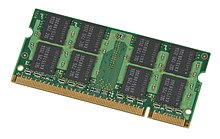
Front and back of a 2GB PC2-5300 DDR2 RAM module for desktop PCs (DIMM)
342:
DDR2's bus frequency is boosted by electrical interface improvements,
1807:
1692:
1153:
17:
1570:
DDR2 low latency vs high bandwidth, Core 2 Duo (Conroe) performance
1815:
1760:
1755:
1722:
1707:
1687:
1675:
1517:
1497:
JEDEC standard: DDR2 SDRAM Specification: JESD79-2F, November 2009
1408:
1359:
1177:
1171:
1068:
1033:
363:
329:
321:
313:
294:
236:
67:
1848:
1843:
1712:
1702:
481:
391:
248:
1578:
445:
334:
Comparison of memory modules for portable/mobile PCs (SO-DIMM)
41:
1053:
In addition to bandwidth and capacity variants, modules can:
1250:"Samsung Demonstrates World's First DDR 3 Memory Prototype"
217:
Double Data Rate 2 Synchronous
Dynamic Random-Access Memory
34:
Double Data Rate 2 Synchronous
Dynamic Random-Access Memory
398:
have 200 pins and often come identified by an additional
1501:
http://www.jedec.org/standards-documents/docs/jesd-79-2e
1559:
394:
with 240 pins and a single locating notch. Laptop DDR2
1081:
in their designation, whereas non-registered (a.k.a. "
1170:
has since designed the GDDR technology further into
1867:
1834:
1806:
1738:
1634:
1613:
366:package of the previous memory generations such as
326:
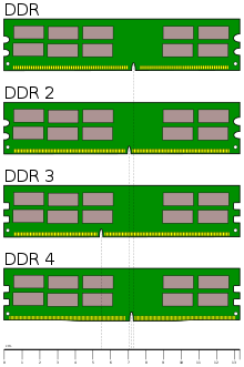
Comparison of memory modules for desktop PCs (DIMM)
204:
194:
182:
170:
157:
147:
135:
109:
91:
83:
73:
59:
747:Relative speed comparison between similar modules
390:For use in computers, DDR2 SDRAM is supplied in
1590:
8:
1526:"DDR2 SDRAM interfaces for next-gen systems"
30:
1198:(definition of "CAS 5-5-5-15", for example)
243:specification, and was itself succeeded by
1597:
1583:
1575:
745:
404:
48:
1549:http://www.jedec.org/standards-documents
229:synchronous dynamic random-access memory
78:Synchronous dynamic random-access memory
1238:
262:In addition to double pumping the data
1432:
1421:
1383:
1372:
1244:
1242:
29:
1450:Mushkin PC2-5300 vs. Corsair PC2-5400
690:
636:
593:
550:
507:
423:
418:
413:
410:
318:PC2-5300 DDR2 SO-DIMM (for notebooks)
7:
1316:. X-bit Laboratories. Archived from
1073:Intel ® 6402 Advanced Memory Buffer
406:Comparison of DDR2 SDRAM standards
1520:Solid State Technology Association
25:
1100:modules, which are designated by
289:DDR2 SDRAM was first produced by
1278:"JEDEC Publishes DDR2 Standard"
1049:DIMM's Notch Positions compared
350:and off-chip drivers. However,
1314:"DDR2 vs. DDR: Revenge gained"
1:
1565:Overview of DDR-II technology
1333:(section 5, tables 15 and 16)
1606:Dynamic random-access memory
1533:Electronic Engineering Times
1402:"SPECIALITY DDR2-1066 SDRAM"
1283:. 2003-09-12. Archived from
1089:identified by an additional
1222:List of interface bit rates
362:package as compared to the
1932:
1353:"DDR2 SDRAM SPECIFICATION"
1506:JEDEC standard: DDR2-1066
1202:Dual-channel architecture
756:
753:
751:
733:
722:
711:
708:
705:
702:
699:
696:
693:
679:
668:
657:
654:
651:
648:
645:
642:
639:
625:
614:
611:
608:
605:
602:
599:
596:
582:
571:
568:
565:
562:
559:
556:
553:
539:
528:
525:
522:
519:
516:
513:
510:
497:
487:
475:
467:
461:
451:
439:
436:
433:
430:
47:
39:
1916:South Korean inventions
1140:Relation to GDDR memory
1431:Cite journal requires
1382:Cite journal requires
1128:Backward compatibility
1074:
1050:
378:available data rates.
335:
327:
319:
293:in 2001. In 2003, the
97:; 21 years ago
1072:
1057:Optionally implement
1037:
333:
325:
317:
1524:Razak Mohammed Ali.
128:DDR2-1066 (PC2-8500)
1467:Samsung Electronics
1411:. November 2007: 70
1312:Ilya Gavrichenkov.
1207:Fully Buffered DIMM
1148:, was developed by
748:
407:
257:backward compatible
125:DDR2-800 (PC2-6400)
122:DDR2-667 (PC2-5333)
119:DDR2-533 (PC2-4266)
116:DDR2-400 (PC2-3200)
36:
1730:Hybrid Memory Cube
1258:. 17 February 2005
1075:
1051:
746:
405:
344:on-die termination
336:
328:
320:
253:forward compatible
1898:
1897:
1217:Registered memory
1144:GDDR2, a form of
1018:
1017:
744:
743:
485:
386:Chips and modules
214:
213:
16:(Redirected from
1923:
1890:Transistor count
1599:
1592:
1585:
1576:
1543:
1541:
1535:. Archived from
1530:
1484:
1483:
1481:
1479:
1474:. 23 August 2003
1458:
1452:
1447:
1441:
1440:
1434:
1429:
1427:
1419:
1417:
1416:
1406:
1398:
1392:
1391:
1385:
1380:
1378:
1370:
1368:
1367:
1362:. April 2008: 78
1357:
1349:
1343:
1340:
1334:
1328:
1322:
1321:
1309:
1303:
1298:
1292:
1291:
1289:
1282:
1274:
1268:
1267:
1265:
1263:
1246:
749:
503:
479:
473:
465:
459:
449:
408:
348:prefetch buffers
277:but with better
225:double data rate
190:
178:
166:
153:
143:
105:
103:
98:
52:
37:
35:
21:
1931:
1930:
1926:
1925:
1924:
1922:
1921:
1920:
1901:
1900:
1899:
1894:
1863:
1830:
1802:
1734:
1682:Fast Cycle DRAM
1630:
1609:
1603:
1556:
1539:
1528:
1523:
1493:
1491:Further reading
1488:
1487:
1477:
1475:
1460:
1459:
1455:
1448:
1444:
1430:
1420:
1414:
1412:
1404:
1400:
1399:
1395:
1381:
1371:
1365:
1363:
1355:
1351:
1350:
1346:
1341:
1337:
1329:
1325:
1311:
1310:
1306:
1299:
1295:
1287:
1280:
1276:
1275:
1271:
1261:
1259:
1248:
1247:
1240:
1235:
1187:
1157:GeForce FX 5800
1142:
1130:
501:
495:
491:
471:
463:
453:
443:
388:
312:
307:
287:
188:
176:
164:
151:
141:
131:
101:
99:
96:
66:
55:
33:
32:
28:
23:
22:
15:
12:
11:
5:
1929:
1927:
1919:
1918:
1913:
1903:
1902:
1896:
1895:
1893:
1892:
1887:
1882:
1880:SDRAM timeline
1877:
1871:
1869:
1865:
1864:
1862:
1861:
1856:
1851:
1846:
1840:
1838:
1836:Memory modules
1832:
1831:
1829:
1828:
1823:
1818:
1812:
1810:
1804:
1803:
1801:
1800:
1799:
1798:
1793:
1788:
1783:
1778:
1773:
1768:
1758:
1753:
1748:
1742:
1740:
1736:
1735:
1733:
1732:
1727:
1726:
1725:
1720:
1715:
1710:
1705:
1695:
1690:
1685:
1679:
1673:
1672:
1671:
1666:
1661:
1656:
1646:
1640:
1638:
1632:
1631:
1629:
1628:
1623:
1617:
1615:
1611:
1610:
1604:
1602:
1601:
1594:
1587:
1579:
1573:
1572:
1567:
1562:
1555:
1554:External links
1552:
1545:
1544:
1542:on 2007-09-26.
1521:
1515:
1509:
1503:
1492:
1489:
1486:
1485:
1453:
1442:
1433:|journal=
1393:
1384:|journal=
1344:
1335:
1331:JEDEC JESD 208
1323:
1320:on 2006-11-21.
1304:
1293:
1290:on 2003-12-04.
1269:
1237:
1236:
1234:
1231:
1230:
1229:
1224:
1219:
1214:
1209:
1204:
1199:
1193:
1186:
1183:
1141:
1138:
1129:
1126:
1125:
1124:
1120:
1111:
1110:
1098:fully buffered
1094:
1066:
1016:
1015:
1012:
1009:
1006:
1003:
1000:
999:PC2-8500 5-5-5
996:
995:
992:
989:
986:
983:
980:
979:PC2-8500 6-6-6
976:
975:
972:
969:
966:
963:
960:
959:PC2-8500 7-7-7
956:
955:
952:
949:
946:
943:
940:
939:PC2-6400 4-4-4
936:
935:
932:
929:
926:
923:
920:
919:PC2-6400 5-5-5
916:
915:
912:
909:
906:
903:
900:
899:PC2-6400 6-6-6
896:
895:
892:
889:
886:
883:
880:
879:PC2-5300 4-4-4
876:
875:
872:
869:
866:
863:
860:
859:PC2-5300 5-5-5
856:
855:
852:
849:
846:
843:
840:
839:PC2-4200 3-3-3
836:
835:
832:
829:
826:
823:
820:
819:PC2-4200 4-4-4
816:
815:
812:
809:
806:
803:
800:
799:PC2-3200 3-3-3
796:
795:
792:
789:
786:
783:
780:
779:PC2-3200 4-4-4
776:
775:
772:
769:
766:
763:
759:
758:
755:
752:
742:
741:
738:
735:
731:
730:
727:
724:
720:
719:
716:
713:
710:
707:
704:
701:
698:
695:
692:
688:
687:
684:
681:
677:
676:
673:
670:
666:
665:
662:
659:
656:
653:
650:
647:
644:
641:
638:
634:
633:
630:
627:
623:
622:
619:
616:
613:
610:
607:
604:
601:
598:
595:
591:
590:
587:
584:
580:
579:
576:
573:
570:
567:
564:
561:
558:
555:
552:
548:
547:
544:
541:
537:
536:
533:
530:
527:
524:
521:
518:
515:
512:
509:
505:
504:
496:
493:
489:
486:
474:
466:
460:
450:
438:
435:
432:
428:
427:
422:
417:
412:
387:
384:
311:
308:
306:
303:
286:
283:
255:with DDR3 nor
247:in 2007. DDR2
212:
211:
206:
202:
201:
196:
192:
191:
186:
180:
179:
174:
168:
167:
162:
155:
154:
149:
145:
144:
139:
133:
132:
130:
129:
126:
123:
120:
117:
113:
111:
107:
106:
102:September 2003
95:September 2003
93:
89:
88:
87:2nd generation
85:
81:
80:
75:
71:
70:
61:
57:
56:
53:
45:
44:
26:
24:
14:
13:
10:
9:
6:
4:
3:
2:
1928:
1917:
1914:
1912:
1909:
1908:
1906:
1891:
1888:
1886:
1883:
1881:
1878:
1876:
1875:DRAM timeline
1873:
1872:
1870:
1866:
1860:
1857:
1855:
1852:
1850:
1847:
1845:
1842:
1841:
1839:
1837:
1833:
1827:
1824:
1822:
1819:
1817:
1814:
1813:
1811:
1809:
1805:
1797:
1794:
1792:
1789:
1787:
1784:
1782:
1779:
1777:
1774:
1772:
1769:
1767:
1764:
1763:
1762:
1759:
1757:
1754:
1752:
1749:
1747:
1744:
1743:
1741:
1737:
1731:
1728:
1724:
1721:
1719:
1716:
1714:
1711:
1709:
1706:
1704:
1701:
1700:
1699:
1696:
1694:
1691:
1689:
1686:
1683:
1680:
1677:
1674:
1670:
1667:
1665:
1662:
1660:
1657:
1655:
1652:
1651:
1650:
1647:
1645:
1642:
1641:
1639:
1637:
1633:
1627:
1624:
1622:
1619:
1618:
1616:
1612:
1607:
1600:
1595:
1593:
1588:
1586:
1581:
1580:
1577:
1571:
1568:
1566:
1563:
1561:
1560:JEDEC website
1558:
1557:
1553:
1551:
1550:
1538:
1534:
1527:
1522:
1519:
1516:
1513:
1510:
1507:
1504:
1502:
1498:
1495:
1494:
1490:
1473:
1469:
1468:
1463:
1457:
1454:
1451:
1446:
1443:
1438:
1425:
1410:
1403:
1397:
1394:
1389:
1376:
1361:
1358:. JESD79-2E.
1354:
1348:
1345:
1339:
1336:
1332:
1327:
1324:
1319:
1315:
1308:
1305:
1302:
1297:
1294:
1286:
1279:
1273:
1270:
1257:
1256:
1251:
1245:
1243:
1239:
1232:
1228:
1225:
1223:
1220:
1218:
1215:
1213:
1210:
1208:
1205:
1203:
1200:
1197:
1194:
1192:
1189:
1188:
1184:
1182:
1179:
1175:
1173:
1169:
1165:
1162:
1158:
1155:
1151:
1147:
1139:
1137:
1134:
1127:
1121:
1118:
1117:
1116:
1115:
1107:
1103:
1099:
1095:
1092:
1088:
1084:
1080:
1071:
1067:
1064:
1060:
1056:
1055:
1054:
1048:
1045:
1041:
1036:
1032:
1029:
1025:
1024:
1013:
1010:
1007:
1004:
1001:
998:
997:
993:
990:
987:
984:
981:
978:
977:
973:
970:
967:
964:
961:
958:
957:
953:
950:
947:
944:
941:
938:
937:
933:
930:
927:
924:
921:
918:
917:
913:
910:
907:
904:
901:
898:
897:
893:
890:
887:
884:
881:
878:
877:
873:
870:
867:
864:
861:
858:
857:
853:
850:
847:
844:
841:
838:
837:
833:
830:
827:
824:
821:
818:
817:
813:
810:
807:
804:
801:
798:
797:
793:
790:
787:
784:
781:
778:
777:
773:
770:
767:
764:
761:
760:
750:
739:
736:
732:
728:
725:
721:
717:
714:
689:
685:
682:
678:
674:
671:
667:
663:
660:
635:
631:
628:
624:
620:
617:
592:
588:
585:
581:
577:
574:
549:
545:
542:
538:
534:
531:
506:
500:
483:
478:
470:
469:Transfer rate
457:
447:
442:
429:
426:
421:
416:
409:
403:
401:
397:
393:
385:
383:
379:
375:
373:
369:
365:
361:
356:
353:
349:
345:
340:
332:
324:
316:
309:
305:Specification
304:
302:
298:
296:
292:
284:
282:
280:
276:
271:
269:
265:
260:
258:
254:
250:
246:
242:
238:
234:
230:
226:
222:
218:
210:
207:
203:
200:
197:
193:
187:
185:
181:
177:400–1066 MT/s
175:
173:
172:Transfer rate
169:
163:
160:
156:
150:
146:
140:
138:
134:
127:
124:
121:
118:
115:
114:
112:
108:
94:
90:
86:
82:
79:
76:
72:
69:
65:
62:
58:
51:
46:
43:
38:
19:
1678:(Mobile DDR)
1653:
1614:Asynchronous
1546:
1537:the original
1532:
1476:. Retrieved
1465:
1456:
1445:
1424:cite journal
1413:. Retrieved
1396:
1375:cite journal
1364:. Retrieved
1347:
1338:
1326:
1318:the original
1307:
1296:
1285:the original
1272:
1260:. Retrieved
1253:
1176:
1143:
1135:
1131:
1113:
1112:
1105:
1101:
1090:
1086:
1078:
1062:
1052:
1046:
1043:
1039:
1027:
1026:
1021:
1019:
399:
389:
380:
376:
357:
341:
337:
299:
288:
272:
268:clock signal
261:
251:are neither
220:
216:
215:
92:Release date
1636:Synchronous
1196:CAS latency
499:CAS latency
462:Clock rate
452:Cycle time
195:Predecessor
165:200–533 MHz
142:100–266 MHz
1905:Categories
1415:2009-03-14
1366:2009-03-14
1233:References
1227:DDR3 SDRAM
1161:colloquial
1146:GDDR SDRAM
1109:insertion.
1083:unbuffered
697:PC2-8500*
691:DDR2-1066
600:PC2-5300*
557:PC2-4200*
441:Clock rate
259:with DDR.
245:DDR3 SDRAM
235:. It is a
221:DDR2 SDRAM
209:DDR3 SDRAM
161:clock rate
152:10–3.75 ns
148:Cycle time
137:Clock rate
84:Generation
31:DDR2 SDRAM
1885:Bandwidth
1826:XDR2 DRAM
1649:DDR SDRAM
1191:DDR SDRAM
1096:Be aware
686:12 or 15
643:PC2-6400
637:DDR2-800
632:12 or 15
594:DDR2-667
551:DDR2-533
514:PC2-3200
508:DDR2-400
477:Bandwidth
431:Standard
372:SDR SDRAM
368:DDR SDRAM
275:bandwidth
241:DDR SDRAM
233:interface
205:Successor
199:DDR SDRAM
110:Standards
60:Developer
1821:XDR DRAM
1739:Graphics
1626:EDO DRAM
1621:FPM DRAM
1255:Phys.org
1185:See also
1164:misnomer
757:PC-6400
754:PC-5300
396:SO-DIMMs
310:Overview
231:(SDRAM)
40:Type of
1854:UniDIMM
1718:HBM-PIM
1684:(FCRAM)
1478:26 June
1472:Samsung
1262:23 June
1212:SO-DIMM
1150:Samsung
1085:") RAM
740:13.125
437:Module
425:Timings
352:latency
291:Samsung
285:History
279:latency
223:) is a
184:Voltage
100: (
64:Samsung
1808:Rambus
1693:RLDRAM
1608:(DRAM)
1154:Nvidia
1087:may be
1047:Server
774:4-4-4
771:5-5-5
768:6-6-6
765:4-4-4
762:5-5-5
737:7-7-7
729:11.25
726:6-6-6
718:9.375
715:5-5-5
683:6-6-6
672:5-5-5
661:4-4-4
629:5-5-5
618:4-4-4
586:4-4-4
578:11.25
575:3-3-3
543:4-4-4
532:3-3-3
472:(MT/s)
227:(DDR)
1911:SDRAM
1868:Lists
1816:RDRAM
1796:GDDR7
1791:GDDR6
1786:GDDR5
1781:GDDR4
1776:GDDR3
1771:GDDR2
1761:SGRAM
1756:MDRAM
1723:HBM3E
1708:HBM2E
1688:eDRAM
1676:LPDDR
1644:SDRAM
1540:(PDF)
1529:(PDF)
1518:JEDEC
1409:JEDEC
1405:(PDF)
1360:JEDEC
1356:(PDF)
1288:(PDF)
1281:(PDF)
1178:GDDR3
1172:GDDR3
1114:Note:
1038:DDR2
1028:Note:
1023:name.
712:8533
709:1066
703:3.75
675:12.5
658:6400
615:5333
572:4266
529:3200
464:(MHz)
434:Type
411:Name
392:DIMMs
364:TSSOP
295:JEDEC
249:DIMMs
237:JEDEC
189:1.8 V
68:JEDEC
18:DDR-2
1859:CAMM
1849:DIMM
1844:SIMM
1766:GDDR
1751:WRAM
1746:VRAM
1713:HBM3
1703:HBM2
1669:DDR5
1664:DDR4
1659:DDR3
1654:DDR2
1480:2019
1437:help
1388:help
1264:2019
1011:−24%
1008:−37%
988:−25%
968:−12%
951:−20%
948:−33%
928:−16%
911:+20%
888:−19%
871:+21%
848:−24%
831:+21%
811:+20%
791:+60%
788:+33%
706:533
700:266
655:800
652:400
646:200
612:667
609:333
603:166
569:533
566:266
563:7.5
560:133
526:400
523:200
517:100
502:(ns)
488:CL-T
482:MB/s
415:Chip
370:and
74:Type
1698:HBM
1499:**
1168:ATI
1104:or
1059:ECC
1042:vs
991:−9%
971:+6%
891:−3%
851:−9%
664:10
621:12
589:12
546:20
535:15
520:10
490:RCD
446:MHz
420:Bus
360:BGA
264:bus
159:Bus
42:RAM
1907::
1531:.
1514:**
1508:**
1470:.
1464:.
1428::
1426:}}
1422:{{
1407:.
1379::
1377:}}
1373:{{
1252:.
1241:^
1106:FB
1020:*
1014:%
994:%
974:%
954:%
934:%
914:%
894:%
874:%
854:%
834:%
814:%
794:%
734:F
723:E
694:D
680:E
669:D
649:5
640:C
626:D
606:6
597:C
583:C
554:B
540:C
511:B
494:RP
492:-T
456:ns
346:,
1598:e
1591:t
1584:v
1482:.
1439:)
1435:(
1418:.
1390:)
1386:(
1369:.
1266:.
1102:F
1091:U
1079:R
1063:P
1044:F
1040:P
1005:%
1002:%
985:%
982:%
965:%
962:%
945:%
942:%
931:=
925:%
922:%
908:=
905:%
902:%
885:%
882:%
868:=
865:%
862:%
845:%
842:%
828:=
825:%
822:%
808:=
805:%
802:%
785:%
782:%
484:)
480:(
458:)
454:(
448:)
444:(
400:S
219:(
104:)
20:)
Text is available under the Creative Commons Attribution-ShareAlike License. Additional terms may apply.