563:, a diode or simple logic components such as flip-flops, or logic gates with multiple inputs. The use of standard cells allows the chip's design to be split into logical and physical levels. A fabless company would normally only work on the logical design of a chip, determining how cells are connected and the functionality of the chip, while following design rules from the foundry the chip will be made in, while the physical design of the chip, the cells themselves, are normally done by the foundry and it comprises the physics of the transistor devices and how they are connected to form a logic gate. Standard cells allow chips to be designed and modified more quickly to respond to market demands, but this comes at the cost of lower transistor density in the chip and thus larger die sizes.
94:
806:, and so on. Verification such as that done by emulators can be carried out in FPGAs or special processors, and emulation replaced simulation. Simulation was initially done by simulating logic gates in chips but later on, RTLs in chips were simulated instead. Simulation is still used when creating analog chip designs. Prototyping platforms are used to run software on prototypes of the chip design while it is under development using FPGAs but are slower to iterate on or modify and can't be used to visualize hardware signals as they would appear in the finished design.
944:, usually involving no more than ten transistors and few connections. An iterative trial-and-error process and "overengineering" of device size was often necessary to achieve a manufacturable IC. Reuse of proven designs allowed progressively more complicated ICs to be built upon prior knowledge. When inexpensive computer processing became available in the 1970s, computer programs were written to simulate circuit designs with greater accuracy than practical by hand calculation. The first circuit simulator for analog ICs was called
25:
731:
stage to decide how the chip will operate functionally. This step is where an IC's functionality and design are decided. IC designers will map out the functional requirements, verification testbenches, and testing methodologies for the whole project, and will then turn the preliminary design into a system-level specification that can be simulated with simple models using languages like C++ and MATLAB and emulation tools. For pure and new designs, the system design stage is where an
303:
826:
1042:
570:(PDK) may be provided by the foundry and it may include the standard cell library as well as the specifications of the cells, and tools to verify the fabless company's design against the design rules specified by the foundry as well as simulate it using the foundry's cells. PDKs may be provided under non-disclosure agreements. Macros/Macrocells/Macro blocks,
956:
design styles – top-down and bottom-up. The top-down design style makes use of optimization-based tools similar to conventional digital flows. Bottom-up procedures re-use “expert knowledge” with the result of solutions previously conceived and captured in a procedural description, imitating an expert's decision. An example are cell generators, such as
82:
586:(IC) development process starts with defining product requirements, progresses through architectural definition, implementation, bringup and finally production. The various phases of the integrated circuit development process are described below. Although the phases are presented here in a straightforward fashion, in reality there is
833:
RTL is only a behavioral model of the actual functionality of what the chip is supposed to operate under. It has no link to a physical aspect of how the chip would operate in real life at the materials, physics, and electrical engineering side. For this reason, the next step in the IC design process,
730:
The initial chip design process begins with system-level design and microarchitecture planning. Within IC design companies, management and often analytics will draft a proposal for a design team to start the design of a new chip to fit into an industry segment. Upper-level designers will meet at this
289:
damage to the tiny components are also of concern. Finally, the physical layout of certain circuit subblocks is typically critical, in order to achieve the desired speed of operation, to segregate noisy portions of an IC from quiet portions, to balance the effects of heat generation across the IC, or
712:
Once a design is mature and has reached mass production it must be sustained. The process must be continually monitored and problems dealt with quickly to avoid a significant impact on production volumes. The goal of sustaining is to maintain production volumes and continually reduce costs until the
699:
Productization is the task of taking a design from engineering into mass production manufacturing. Although a design may have successfully met the specifications of the product in the lab during the bringup phase there are many challenges that product engineers face when trying to mass-produce those
645:
The micro-architecture is a step closer to the hardware. It implements the architecture and defines specific mechanisms and structures for achieving that implementation. The result of the micro-architecture phase is a micro-architecture specification which describes the methods used to implement the
632:
defines the fundamental structure, goals and principles of the product. It defines high level concepts and the intrinsic value proposition of the product. Architecture teams take into account many variables and interface with many groups. People creating the architecture generally have a significant
968:
A challenge most critical to analog IC design involves the variability of the individual devices built on the semiconductor chip. Unlike board-level circuit design which permits the designer to select devices that have each been tested and binned according to value, the device values on an IC can
973:
can vary from 20 to 100. In the latest CMOS processes, β of vertical PNP transistors can even go below 1. To add to the design challenge, device properties often vary between each processed semiconductor wafer. Device properties can even vary significantly across each individual IC due to doping
955:
As many functional constraints must be considered in analog design, manual design is still widespread today, in contrast to digital design which is highly automated, including automated routing and synthesis. As a result, modern design flows for analog circuits are characterized by two different
978:. The underlying cause of this variability is that many semiconductor devices are highly sensitive to uncontrollable random variances in the process. Slight changes to the amount of diffusion time, uneven doping levels, etc. can have large effects on device properties.
781:
To reduce the number of functionality bugs, a separate hardware verification group will take the RTL and design testbenches and systems to check that the RTL actually is performing the same steps under many different conditions, classified as the domain of
905:: The design is modified, where possible, to make it as easy and efficient as possible to produce. This is achieved by adding extra vias or adding dummy metal/diffusion/poly layers wherever possible while complying to the design rules set by the foundry.
555:
Note that the second step, RTL design, is responsible for the chip doing the right thing. The third step, physical design, does not affect the functionality at all (if done correctly) but determines how fast the chip operates and how much it costs.
841:
The main steps of physical design are listed below. In practice there is not a straightforward progression - considerable iteration is required to ensure all objectives are met simultaneously. This is a difficult problem in its own right, called
236:
is the design, test, and verification of the instructions that the IC is to carry out. Artificial
Intelligence has been demonstrated in chip design for creating chip layouts which are the locations of standard cells and macro blocks in a chip.
222:
for what can and cannot be manufactured are also extremely complex. Common IC processes of 2015 have more than 500 rules. Furthermore, since the manufacturing process itself is not completely predictable, designers must account for its
1080:
686:
are performed starting from very simple tests such as ensuring that the device will power on to much more complicated tests which try to stress the part in various ways. The result of the bringup phase is documentation of
774:, RTL designers will break a functional description into hardware models of components on the chip working together. Each of the simple statements described in the system design can easily turn into thousands of lines of
88:
of a simple CMOS Operational
Amplifier (inputs are to the left and the compensation capacitor is to the right). The metal layer is coloured blue, green and brown are N- and P-doped Si, the polysilicon is red and vias are
187:. Digital design focuses on logical correctness, maximizing circuit density, and placing circuits so that clock and timing signals are routed efficiently. Analog IC design also has specializations in power IC design and
231:
in the IC design process. The design of some processors has become complicated enough to be difficult to fully test, and this has caused problems at large cloud providers. In short, the design of an IC using
813:
caused the results of a division to be wrong by at most 61 parts per million, in cases that occurred very infrequently. No one even noticed it until the chip had been in production for months. Yet
940:
Before the advent of the microprocessor and software based design tools, analog ICs were designed using hand calculations and process kit parts. These ICs were low complexity circuits, for example,
215:. Fidelity of analog signal amplification and filtering is usually critical, and as a result analog ICs use larger area active devices than digital designs and are usually less dense in circuitry.
948:(Simulation Program with Integrated Circuits Emphasis). Computerized circuit simulation tools enable greater IC design complexity than hand calculations can achieve, making the design of analog
574:
and IP blocks have greater functionality than standard cells, and are used similarly. There are soft macros and hard macros. Standard cells are usually placed following standard cell rows.
1304:
838:
stage, is to map the RTL into actual geometric representations of all electronics devices, such as capacitors, resistors, logic gates, and transistors that will go on the chip.
566:
Foundries supply libraries of standard cells to fabless companies, for design purposes and to allow manufacturing of their designs using the foundry's facilities. A
770:. Using digital design components like adders, shifters, and state machines as well as computer architecture concepts like pipelining, superscalar execution, and
704:
must be ramped up to production volumes with an acceptable yield. The goal of the productization phase is to reach mass production volumes at an acceptable cost.
633:
amount of experience dealing with systems in the area for which the architecture is being created. The work product of the architecture phase is an architectural
735:
and operation is planned out, and in most chips existing instruction sets are modified for newer functionality. Design at this stage is often statements such as
499:
design: This step creates the user functional specification. The user may use a variety of languages and tools to create this description. Examples include a
1111:
1055:
859:: The RTL of the chip is assigned to gross regions of the chip, input/output (I/O) pins are assigned and large objects (arrays, cores, etc.) are placed.
678:
After a design is created, taped-out and manufactured, actual hardware, 'first silicon', is received which is taken into the lab where it goes through
1143:
778:
code, which is why it is extremely difficult to verify that the RTL will do the right thing in all the possible cases that the user may throw at it.
654:
In the implementation phase the design itself is created using the micro-architectural specification as the starting point. This involves low level
537:(RTL) description. The RTL describes the exact behavior of the digital circuits on the chip, as well as the interconnections to inputs and outputs.
551:, layout and floor planning, figuring out which gates to use, defining places for them, and wiring (clock timing synthesis, routing) them together.
949:
184:
269:
is necessary since the substrate silicon is conductive and often forms an active region of the individual components. The two common methods are
379:
1408:
1351:
1215:
212:
750:. At later stages in the design process, each of these innocent looking statements expands to hundreds of pages of textual documentation.
46:
258:
277:. Attention must be given to power dissipation of transistors and interconnect resistances and current density of the interconnect,
1509:
902:
896:
352:
68:
227:
nature. The complexity of modern IC design, as well as market pressure to produce designs rapidly, has led to the extensive use of
1539:
211:. Analog design is more concerned with the physics of the semiconductor devices such as gain, matching, power dissipation, and
758:
Upon agreement of a system design, RTL designers then implement the functional models in a hardware description language like
93:
1231:
Tokuda, T.; Korematsu, J.; Shimazu, Y.; Sakashita, N.; Kengaku, T.; Fugiyama, T.; Ohno, T.; Tomisawa, O. (December 7, 1988).
746:
1205:
969:
vary widely which are uncontrollable by the designer. For example, some IC resistors can vary ±20% and β of an integrated
835:
615:
540:
1276:
817:
was forced to offer to replace, for free, every chip sold until they could fix the bug, at a cost of $ 475 million (US).
218:
Modern ICs are enormously complicated. An average desktop computer chip, as of 2015, has over 1 billion transistors. The
1529:
1513:
1065:
1015:
856:
423:
357:
233:
228:
1001:
device layout to cancel variations in devices which must match closely (such as the transistor differential pair of an
868:
Logic/placement refinement: Iterative logical and placement transformations to close performance and power constraints.
1085:
970:
909:
871:
464:
39:
33:
1432:
Basu, Joydeep (2019-10-09). "From Design to Tape-out in SCL 180 nm CMOS Integrated
Circuit Fabrication Technology".
991:
Making devices large so that statistical variations become an insignificant fraction of the overall device property.
1534:
908:
Final checking: Since errors are expensive, time-consuming and hard to spot, extensive error checking is the rule,
519:
1070:
1060:
418:
85:
1477:
50:
500:
281:
since ICs contain very tiny devices compared to discrete components, where such concerns are less of an issue.
1262:
1130:"FYI: Today's computer chips are so advanced, they are more 'mercurial' than precise – and here's the proof"
783:
775:
534:
496:
433:
286:
121:
688:
1023:
274:
270:
1374:
928:
799:
714:
392:
1290:
998:
913:
172:
137:
1318:
994:
Segmenting large devices, such as resistors, into parts and interweaving them to cancel variations.
266:
133:
533:
RTL design: This step converts the user specification (what the user wants the chip to do) into a
1459:
1441:
1414:
1357:
1047:
795:
701:
682:. Bringup is the process of powering, testing and characterizing the design in the lab. Numerous
607:
583:
567:
348:
160:
141:
97:
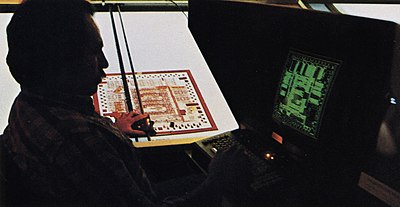
Engineer using an early IC-designing workstation to analyze a section of a circuit design cut on
1505:
1404:
1347:
1211:
771:
278:
200:
1451:
1396:
1339:
1244:
1129:
1075:
892:
810:
787:
548:
481:
469:
282:
196:
176:
149:
1390:
1333:
985:
Using the ratios of resistors, which do match closely, rather than absolute resistor value.
302:
1027:
862:
850:
786:. Many techniques are used, none of them perfect but all of them useful – extensive
732:
683:
571:
291:
188:
164:
1144:"Now Google is using AI to design chips, far faster than human engineers can do the job"
611:
888:
843:
791:
129:
1523:
1463:
1418:
1361:
1090:
881:
865:: The gates in the netlist are assigned to nonoverlapping locations on the die area.
803:
763:
634:
544:
516:
428:
208:
145:
125:
853:: The RTL is mapped into a gate-level netlist in the target technology of the chip.
628:
599:
219:
180:
156:
1455:
825:
245:
Integrated circuit design involves the creation of electronic components, such as
1164:
1277:"Processors to Emulate Processors: The Palladium II | the CPU Shack Museum"
603:
246:
1332:
J. Lienig, J. Scheible (2020). "Chap. 3.3: Mask Data: Layout Post
Processing".
1041:
981:
Some design techniques used to reduce the effects of the device variation are:
1400:
1343:
1037:
988:
Using devices with matched geometrical shapes so they have matched variations.
875:
655:
560:
254:
224:
204:
1389:
J. Lienig, J. Scheible (2020). "Chap. 4.6: Analog and
Digital Design Flows".
1237:
IEEE Transactions on
Computer-Aided Design of Integrated Circuits and Systems
1232:
1081:
IEEE Transactions on
Computer-Aided Design of Integrated Circuits and Systems
975:
924:
587:
484:
may be used during chip development to establish new connections in a chip.
250:
1019:
920:
809:
A tiny error here can make the whole chip useless, or worse. The famous
667:
523:
399:
98:
759:
691:(how well the part performs to spec) and errata (unexpected behavior).
512:
262:
81:
1375:
https://www-group.slac.stanford.edu/ais/publicDocs/presentation137.pdf
1165:"Inside Intel: here's what goes into making a cutting-edge gaming CPU"
475:
Plan for next generation chip using production information if possible
1248:
1183:
1112:"Analog IC: Understanding Its Importance, Functions and Applications"
1002:
941:
663:
527:
192:
1446:
1305:"Cadence Strikes Back at Synopsys with New Circuit Simulation Tool"
543:: This step takes the RTL, and a library of available logic gates (
504:
492:
Roughly saying, digital IC design can be divided into three parts.
1148:
957:
945:
824:
814:
602:
can be defined some high level product goals must be defined. The
301:
767:
659:
606:
are usually generated by a cross functional team that addresses
508:
168:
662:, entering schematics and verification. This phase ends with a
547:
library), and creates a chip design. This step involves use of
914:
checking that the manufacturing rules were followed faithfully
738:
451:
265:. A method to isolate the individual components formed in the
163:
IC design. Digital IC design is to produce components such as
18:
1502:
Electronic Design
Automation For Integrated Circuits Handbook
261:
of these components onto a piece of semiconductor, typically
884:: The wires that connect the gates in the netlist are added.
155:
IC design can be divided into the broad categories of
1392:
Fundamentals of Layout Design for
Electronic Circuits
1335:
Fundamentals of Layout Design for
Electronic Circuits
191:
IC design. Analog IC design is used in the design of
923:
and mask generation: the design data is turned into
829:
Physical design steps within the digital design flow
910:
making sure the mapping to logic was done correctly
310:A typical IC design cycle involves several steps:
1233:"A macrocell approach for VLSI processor design"
1516:, one of the main enablers of modern IC design.
614:, and much more. This phase should result in a
1384:
1382:
337:System simulation, emulation, and verification
559:A standard cell normally represents a single
8:
294:of connections to circuitry outside the IC.
1056:Integrated circuit layout design protection
16:Engineering process for electronic hardware
590:and these steps may occur multiple times.
1445:
1184:"Inside Intel: From Silicon to the World"
726:Microarchitecture and system-level design
69:Learn how and when to remove this message
92:
80:
32:This article includes a list of general
1102:
887:Postwiring optimization: Performance (
331:Analogue design, simulation, and layout
317:Feasibility study and die size estimate
136:, or ICs. ICs consist of miniaturized
1199:
1197:
7:
1504:, by Lavagno, Martin, and Scheffer,
1263:"Cadence Introduces Palladium XP II"
1014:The three largest companies selling
874:: Clock signal wiring is (commonly,
325:Architectural or system-level design
463:Yield analysis / warranty analysis
1478:"Developments of Multi-CAD Models"
1163:Jacob Ridley (December 26, 2022).
38:it lacks sufficient corresponding
14:
353:automatic test pattern generation
306:Major steps in the IC design flow
1204:Chen, Wai-Kai (3 October 2018).
1040:
450:Datasheet generation (usually a
23:
1319:"The First Emulators of Spring"
1395:. Springer. pp. 151–159.
1338:. Springer. pp. 102–110.
1118:– via www.quarktwin.com.
1110:Parker Brakus (May 17, 2022).
878:) introduced into the design.
747:IEEE floating-point arithmetic
132:techniques required to design
124:, encompassing the particular
1:
1456:10.1080/09747338.2019.1657787
1291:"Transaction-based Emulation"
616:product requirements document
334:Digital design and simulation
285:in metallic interconnect and
1514:electronic design automation
1171:– via www.pcgamer.com.
1066:Electronic design automation
1016:electronic design automation
903:Design for manufacturability
897:Design for manufacturability
358:Design for manufacturability
1086:Multi-project wafer service
1556:
658:and partitioning, writing
407:Layout-to-mask preparation
378:Physical verification and
1512:A survey of the field of
1485:IC CAD Market Trends 2015
1434:IETE Journal of Education
1401:10.1007/978-3-030-39284-0
1344:10.1007/978-3-030-39284-0
1071:Power network design (IC)
1061:Electronic circuit design
899:) violations are removed.
395:(layout post-processing)
106:Integrated circuit design
1251:– via IEEE Xplore.
520:Transaction Level Models
387:Co-simulation and timing
345:Digital design synthesis
964:Coping with variability
784:functional verification
541:Physical circuit design
535:register transfer level
497:Electronic system-level
439:Device characterization
434:Post silicon validation
122:electronics engineering
53:more precise citations.
1540:Electronic engineering
830:
307:
271:p-n junction isolation
229:automated design tools
102:
90:
929:mask data preparation
828:
802:-like code checking,
689:characterization data
415:Photomask fabrication
393:Mask data preparation
314:System specification
305:
138:electronic components
96:
84:
919:Chip finishing with
442:Tweak (if necessary)
398:Chip finishing with
373:Parasitic extraction
275:dielectric isolation
120:, is a sub-field of
110:semiconductor design
1530:Integrated circuits
1265:. 18 February 2024.
1182:Shimpi, Anand Lal.
412:Reticle fabrication
134:integrated circuits
1279:. 21 October 2016.
1048:Electronics portal
831:
796:hardware emulation
641:Micro-architecture
610:, customer needs,
608:market opportunity
584:integrated circuit
568:Process design kit
349:Design for testing
308:
290:to facilitate the
201:phase locked loops
142:electrical network
103:
91:
1535:Electronic design
1410:978-3-030-39284-0
1353:978-3-030-39284-0
1243:(12): 1272–1277.
1217:978-1-4200-0596-7
1207:The VLSI Handbook
1188:www.anandtech.com
772:branch prediction
482:Focused ion beams
419:Wafer fabrication
320:Function analysis
279:contacts and vias
197:linear regulators
79:
78:
71:
1547:
1489:
1488:
1482:
1474:
1468:
1467:
1449:
1429:
1423:
1422:
1386:
1377:
1372:
1366:
1365:
1329:
1323:
1322:
1321:. 13 April 2021.
1315:
1309:
1308:
1301:
1295:
1294:
1293:. 24 March 2024.
1287:
1281:
1280:
1273:
1267:
1266:
1259:
1253:
1252:
1249:10.1109/43.16805
1228:
1222:
1221:
1201:
1192:
1191:
1179:
1173:
1172:
1160:
1154:
1153:
1140:
1134:
1133:
1126:
1120:
1119:
1107:
1076:Processor design
1050:
1045:
1044:
893:signal integrity
811:Pentium FDIV bug
788:logic simulation
713:product reaches
578:Design lifecycle
572:Macrocell arrays
549:IC layout editor
470:Failure analysis
447:Chip deployment
364:Physical design
283:Electromigration
150:photolithography
144:on a monolithic
74:
67:
63:
60:
54:
49:this article by
40:inline citations
27:
26:
19:
1555:
1554:
1550:
1549:
1548:
1546:
1545:
1544:
1520:
1519:
1498:
1496:Further reading
1493:
1492:
1480:
1476:
1475:
1471:
1431:
1430:
1426:
1411:
1388:
1387:
1380:
1373:
1369:
1354:
1331:
1330:
1326:
1317:
1316:
1312:
1303:
1302:
1298:
1289:
1288:
1284:
1275:
1274:
1270:
1261:
1260:
1256:
1230:
1229:
1225:
1218:
1203:
1202:
1195:
1181:
1180:
1176:
1162:
1161:
1157:
1142:
1141:
1137:
1128:
1127:
1123:
1109:
1108:
1104:
1099:
1046:
1039:
1036:
1028:Mentor Graphics
1012:
999:common centroid
966:
938:
872:Clock insertion
851:Logic synthesis
836:physical design
823:
821:Physical design
756:
737:encodes in the
733:Instruction set
728:
723:
710:
697:
676:
652:
643:
624:
596:
580:
490:
436:and integration
370:Place and route
342:Circuit design
300:
259:interconnection
243:
165:microprocessors
75:
64:
58:
55:
45:Please help to
44:
28:
24:
17:
12:
11:
5:
1553:
1551:
1543:
1542:
1537:
1532:
1522:
1521:
1518:
1517:
1497:
1494:
1491:
1490:
1469:
1424:
1409:
1378:
1367:
1352:
1324:
1310:
1307:. 21 May 2021.
1296:
1282:
1268:
1254:
1223:
1216:
1193:
1174:
1155:
1135:
1121:
1101:
1100:
1098:
1095:
1094:
1093:
1088:
1083:
1078:
1073:
1068:
1063:
1058:
1052:
1051:
1035:
1032:
1011:
1008:
1007:
1006:
995:
992:
989:
986:
965:
962:
937:
934:
933:
932:
917:
906:
900:
895:), and yield (
889:timing closure
885:
879:
869:
866:
860:
854:
844:design closure
822:
819:
792:formal methods
755:
752:
727:
724:
722:
721:Design process
719:
709:
706:
696:
695:Productization
693:
675:
672:
651:
650:Implementation
648:
646:architecture.
642:
639:
623:
620:
595:
592:
579:
576:
553:
552:
538:
531:
489:
486:
479:
478:
477:
476:
473:
472:on any returns
467:
461:
458:
455:
445:
444:
443:
440:
437:
426:
421:
416:
413:
410:
409:
408:
405:
404:Reticle layout
402:
390:
389:
388:
385:
376:
375:
374:
371:
368:
362:
361:
360:
355:
346:
340:
339:
338:
335:
332:
326:
323:
322:
321:
318:
299:
296:
242:
239:
209:active filters
183:) and digital
140:built into an
130:circuit design
77:
76:
31:
29:
22:
15:
13:
10:
9:
6:
4:
3:
2:
1552:
1541:
1538:
1536:
1533:
1531:
1528:
1527:
1525:
1515:
1511:
1510:0-8493-3096-3
1507:
1503:
1500:
1499:
1495:
1487:. 2015-07-11.
1486:
1479:
1473:
1470:
1465:
1461:
1457:
1453:
1448:
1443:
1439:
1435:
1428:
1425:
1420:
1416:
1412:
1406:
1402:
1398:
1394:
1393:
1385:
1383:
1379:
1376:
1371:
1368:
1363:
1359:
1355:
1349:
1345:
1341:
1337:
1336:
1328:
1325:
1320:
1314:
1311:
1306:
1300:
1297:
1292:
1286:
1283:
1278:
1272:
1269:
1264:
1258:
1255:
1250:
1246:
1242:
1238:
1234:
1227:
1224:
1219:
1213:
1210:. CRC Press.
1209:
1208:
1200:
1198:
1194:
1189:
1185:
1178:
1175:
1170:
1166:
1159:
1156:
1151:
1150:
1145:
1139:
1136:
1131:
1125:
1122:
1117:
1113:
1106:
1103:
1096:
1092:
1091:Standard cell
1089:
1087:
1084:
1082:
1079:
1077:
1074:
1072:
1069:
1067:
1064:
1062:
1059:
1057:
1054:
1053:
1049:
1043:
1038:
1033:
1031:
1029:
1025:
1021:
1017:
1009:
1004:
1000:
996:
993:
990:
987:
984:
983:
982:
979:
977:
972:
963:
961:
959:
953:
951:
947:
943:
936:Analog design
935:
930:
926:
922:
918:
915:
911:
907:
904:
901:
898:
894:
890:
886:
883:
880:
877:
873:
870:
867:
864:
861:
858:
857:Floorplanning
855:
852:
849:
848:
847:
845:
839:
837:
827:
820:
818:
816:
812:
807:
805:
804:code coverage
801:
797:
793:
789:
785:
779:
777:
773:
769:
765:
764:SystemVerilog
761:
753:
751:
749:
748:
742:
740:
734:
725:
720:
718:
716:
707:
705:
703:
700:designs. The
694:
692:
690:
685:
681:
673:
671:
669:
665:
661:
657:
649:
647:
640:
638:
636:
635:specification
631:
630:
621:
619:
617:
613:
609:
605:
601:
593:
591:
589:
585:
577:
575:
573:
569:
564:
562:
557:
550:
546:
545:standard cell
542:
539:
536:
532:
529:
525:
521:
518:
517:SystemVerilog
514:
510:
506:
502:
498:
495:
494:
493:
487:
485:
483:
474:
471:
468:
466:
462:
459:
456:
453:
449:
448:
446:
441:
438:
435:
432:
431:
430:
427:
425:
422:
420:
417:
414:
411:
406:
403:
401:
397:
396:
394:
391:
386:
384:Static timing
383:
382:
381:
377:
372:
369:
367:Floorplanning
366:
365:
363:
359:
356:
354:
350:
347:
344:
343:
341:
336:
333:
330:
329:
328:Logic design
327:
324:
319:
316:
315:
313:
312:
311:
304:
297:
295:
293:
288:
284:
280:
276:
272:
268:
264:
260:
256:
252:
248:
240:
238:
235:
230:
226:
221:
216:
214:
210:
206:
202:
198:
194:
190:
186:
182:
178:
174:
170:
166:
162:
158:
153:
151:
148:substrate by
147:
146:semiconductor
143:
139:
135:
131:
127:
123:
119:
115:
111:
107:
100:
95:
87:
83:
73:
70:
62:
52:
48:
42:
41:
35:
30:
21:
20:
1501:
1484:
1472:
1440:(2): 51–64.
1437:
1433:
1427:
1391:
1370:
1334:
1327:
1313:
1299:
1285:
1271:
1257:
1240:
1236:
1226:
1206:
1187:
1177:
1168:
1158:
1147:
1138:
1124:
1115:
1105:
1013:
980:
967:
954:
952:practical.
939:
840:
832:
808:
780:
757:
744:
736:
729:
711:
698:
679:
677:
653:
644:
629:architecture
627:
625:
622:Architecture
604:requirements
600:architecture
597:
594:Requirements
581:
565:
558:
554:
491:
480:
309:
244:
241:Fundamentals
234:EDA software
217:
171:, memories (
154:
117:
113:
109:
105:
104:
101:, circa 1979
65:
56:
37:
876:clock trees
745:implements
715:end of life
612:feasibility
465:reliability
298:Design flow
247:transistors
225:statistical
205:oscillators
114:chip design
86:Layout view
51:introducing
1524:Categories
1447:1908.10674
1097:References
1018:tools are
925:photomasks
891:), noise (
754:RTL design
708:Sustaining
656:definition
598:Before an
561:logic gate
460:Production
255:capacitors
213:resistance
59:March 2019
34:references
1464:201657819
1419:215840278
1362:215840278
1116:Quarktwin
976:gradients
863:Placement
666:reaching
588:iteration
424:Packaging
292:placement
267:substrate
251:resistors
118:IC design
1169:PC Gamer
1034:See also
1020:Synopsys
524:Simulink
429:Die test
400:tape out
257:and the
99:rubylith
89:crosses.
1024:Cadence
1010:Vendors
942:op-amps
921:Tapeout
882:Routing
760:Verilog
680:bringup
674:Bringup
668:tapeout
513:SystemC
507:model,
488:Summary
457:Ramp up
380:signoff
263:silicon
193:op-amps
157:digital
47:improve
1508:
1462:
1417:
1407:
1360:
1350:
1214:
1026:, and
1003:op amp
997:Using
958:PCells
912:, and
741:format
664:design
528:MATLAB
526:, and
179:, and
161:analog
36:, but
1481:(PDF)
1460:S2CID
1442:arXiv
1415:S2CID
1358:S2CID
1149:ZDNet
950:ASICs
946:SPICE
815:Intel
766:, or
684:tests
454:file)
220:rules
185:ASICs
181:flash
169:FPGAs
126:logic
1506:ISBN
1405:ISBN
1348:ISBN
1212:ISBN
800:lint
768:VHDL
660:code
626:The
582:The
509:VHDL
351:and
273:and
207:and
159:and
128:and
1452:doi
1397:doi
1340:doi
1245:doi
971:BJT
927:in
776:RTL
743:or
739:MP3
505:C++
452:PDF
287:ESD
177:ROM
173:RAM
116:or
1526::
1483:.
1458:.
1450:.
1438:60
1436:.
1413:.
1403:.
1381:^
1356:.
1346:.
1239:.
1235:.
1196:^
1186:.
1167:.
1146:.
1114:.
1030:.
1022:,
1005:).
960:.
846:.
798:,
794:,
790:,
762:,
717:.
702:IC
670:.
637:.
618:.
522:,
515:,
511:,
253:,
249:,
203:,
199:,
195:,
189:RF
175:,
167:,
152:.
112:,
108:,
1466:.
1454::
1444::
1421:.
1399::
1364:.
1342::
1247::
1241:7
1220:.
1190:.
1152:.
1132:.
931:.
916:.
530:.
503:/
501:C
72:)
66:(
61:)
57:(
43:.
Text is available under the Creative Commons Attribution-ShareAlike License. Additional terms may apply.