114:
571:
attributed to the change of volume fraction of surface grains. In addition, the anisotropic properties of each grain become significant with the decrease of workpiece size, which results in the inhomogeneous deformation, irregular formed geometry and the variation of deformation load. There is a critical need to establish the systematic knowledge of microforming to support the design of part, process, and tooling with the consideration of size effects.
20:
105:
410:). The purpose of these thin films depends upon the type of device. Electronic devices may have thin films which are conductors (metals), insulators (dielectrics) or semiconductors. Optical devices may have films which are reflective, transparent, light guiding or scattering. Films may also have a chemical or mechanical purpose as well as for MEMS applications. Examples of deposition techniques include:
554:, and microcutting. These and other microforming processes have been envisioned and researched since at least 1990, leading to the development of industrial- and experimental-grade manufacturing tools. However, as Fu and Chan pointed out in a 2013 state-of-the-art technology review, several issues must still be resolved before the technology can be implemented more widely, including
108:
Simplified illustration of the process of fabrication of a CMOS inverter on p-type substrate in semiconductor microfabrication. Each etch step is detailed in the following image. The diagrams are not to scale, as in real devices, the gate, source, and drain contacts are not normally located in the
393:
can be used. For optical devices or flat panel displays, transparent substrates such as glass or quartz are common. The substrate enables easy handling of the micro device through the many fabrication steps. Often many individual devices are made together on one substrate and then singulated into
691:
Surface preparation is just a different viewpoint, all the steps are the same as described above: it is about leaving the wafer surface in a controlled and well known state before you start processing. Wafers are contaminated by previous process steps (e.g. metals bombarded from chamber walls by
481:
It is often desirable to pattern a film into distinct features or to form openings (or vias) in some of the layers. These features are on the micrometer or nanometer scale and the patterning technology is what defines microfabrication. This patterning technique typically uses a 'mask' to define
570:
to the material volume decreases with the decrease of specimen size and the increase of grain size. This leads to the decrease of grain boundary strengthening effect. Surface grains have lesser constraints compared to internal grains. The change of flow stress with part geometry size is partly
58:/lab-on-a-chip, optical MEMS (also called MOEMS), RF MEMS, PowerMEMS, BioMEMS and their extension into nanoscale (for example NEMS, for nano electro mechanical systems). The production of flat-panel displays and solar cells also uses similar techniques.
253:
size range to micrometer range, but they do not share the main idea of microelectronics-originated microfabrication: replication and parallel fabrication of hundreds or millions of identical structures. This parallelism is present in various
506:
Etching is the removal of some portion of the thin film or substrate. The substrate is exposed to an etching (such as an acid or plasma) which chemically or physically attacks the film until it is removed. Etching techniques include:
77:, ultra-precision engineering, fabrication processes, and equipment design. It is also giving rise to various kinds of interdisciplinary research. The major concepts and principles of microfabrication are
329:) portions of the film. Thin film metrology is used typically during each of these individual process steps, to ensure the film structure has the desired characteristics in terms of thickness (
23:
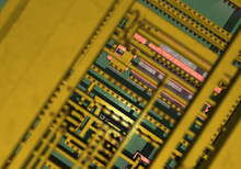
Synthetic detail of a micromanufactured integrated circuit through four layers of planarized copper interconnect, down to the polysilicon (pink), wells (greyish) and substrate (green)
668:
mixture (a.k.a. Piranha) removes organics. Hydrogen fluoride removes native oxide from silicon surface. These are all wet cleaning steps in solutions. Dry cleaning methods include
684:. Pre-gate cleaning is the most critical cleaning step in CMOS fabrication: it ensures that the ca. 2 nm thick oxide of a MOS transistor can be grown in an orderly fashion.
761:
Löper, Philipp; Stuckelberger, Michael; Niesen, Bjoern; Werner, Jérémie; Filipič, Miha; Moon, Soo-Jin; Yum, Jun-Ho; Topič, Marko; De Wolf, Stefaan; Ballif, Christophe (2015).
580:
a wide variety of other processes for cleaning, planarizing, or modifying the chemical properties of microfabricated devices can also be performed. Some examples include:
1011:
1641:
278:
Microfabrication is actually a collection of technologies which are utilized in making microdevices. Some of them have very old origins, not connected to
321:
To fabricate a microdevice, many processes must be performed, one after the other, many times repeatedly. These processes typically include depositing a
1799:
1488:
1713:
463:
1460:
1430:
1364:
1270:
1243:
1216:
1197:
1066:
234:
fabrication and integrated circuit technology are terms used instead of microfabrication, but microfabrication is the broad general term.
1718:
1646:
144:
763:"Complex Refractive Index Spectra of CH3NH3PbI3 Perovskite Thin Films Determined by Spectroscopic Ellipsometry and Spectrophotometry"
1401:
1337:
1318:
1289:
1170:
1143:
1116:
1095:
934:
850:
749:
597:
295:
54:(Japanese terminology) and their subfields have re-used, adapted or extended microfabrication methods. These subfields include
688:, and all high temperature steps are very sensitive to contamination, and cleaning steps must precede high temperature steps.
1703:
1544:
1508:
543:
231:
140:
47:
707:: first they remove all unwanted bits and pieces, and then they reconstruct the desired pattern so that the game can go on.
1708:
1481:
365:
layers that constitute the final device. Modern microprocessors are made with 30 masks while a few masks suffice for a
134:
43:
546:(MEMS) "parts or structures with at least two dimensions in the submillimeter range." It includes techniques such as
1759:
1615:
526:
501:
385:
Microfabricated devices are not generally freestanding devices but are usually formed over or in a thicker support
326:
927:
Micro-scaled
Products Development via Microforming: Deformation Behaviours, Processes, Tooling and its Realization
1450:
726:
555:
520:
447:
424:
315:
227:
1809:
1749:
1474:
903:
357:
steps, and many others are performed. The complexity of microfabrication processes can be described by their
1804:
1534:
648:
Cleanrooms provide passive cleanliness but the wafers are also actively cleaned before every critical step.
551:
311:
1693:
1661:
1592:
584:
458:
354:
82:
1006:
1001:
1597:
645:
are micrometers in size, and their presence will destroy the functionality of a microfabricated device.
1769:
516:
407:
173:
113:
1728:
1698:
716:
588:
386:
223:
150:
130:
970:
453:
342:
299:
267:
165:
61:
Miniaturization of various devices presents challenges in many areas of science and engineering:
39:
190:
1308:
1106:
1426:
1397:
1370:
1360:
1343:
1333:
1314:
1295:
1285:
1266:
1249:
1239:
1222:
1212:
1193:
1166:
1139:
1112:
1091:
1062:
1021:
995:
930:
846:
838:
782:
745:
657:
414:
374:
263:
70:
19:
1077:
1764:
1636:
1418:
1412:
1389:
1383:
1185:
1158:
1131:
1083:
1054:
1048:
962:
882:
814:
774:
693:
592:
486:
346:
207:
78:
74:
953:
Fu, M.W.; Chan, W.L. (2013). "A review on the state-of-the-art microforming technologies".
1513:
1497:
1454:
721:
104:
809:
Engel, U.; Eckstein, R. (2002). "Microforming - From Basic research to its realization".
558:, forming system stability, mechanical properties, and other size-related effects on the
38:
scales and smaller. Historically, the earliest microfabrication processes were used for
1651:
1620:
1569:
1518:
642:
567:
547:
512:
482:
portions of the film which will be removed. Examples of patterning techniques include:
303:
51:
818:
744:
Nitaigour
Premchand Mahalik (2006) "Micromanufacturing and Nanotechnology", Springer,
1793:
974:
704:
661:
390:
377:
photography, with many patterns aligned to each other to create the final structure.
366:
279:
55:
31:
1016:
226:
are in use. Micromachining, semiconductor processing, microelectronic fabrication,
1723:
1035:: Microelectronics and Nanometer Structures: Processing, Measurement, and Phenomena
606:
307:
94:
656:-peroxide solution removes organic contamination and particles; RCA-2 cleaning in
887:
266:
techniques which have successfully been applied in the microregime. For example,
622:
559:
539:
370:
283:
1666:
1587:
1539:
1357:
Ultraclean
Surface Processing of Silicon Wafers: Secrets of VLSI Manufacturing
1189:
1135:
966:
250:
184:
160:
86:
35:
1448:
Videos and animations on microfabrication techniques and related applications
1374:
1226:
1774:
1347:
1299:
1253:
685:
649:
618:
403:
322:
291:
194:
180:
98:
66:
786:
703:
Wafer cleaning and surface preparation work similarly to the machines in a
1422:
1162:
1087:
1058:
870:
1656:
1579:
677:
665:
638:
626:
255:
219:
325:, patterning the film with the desired micro features, and removing (or
1393:
697:
681:
653:
470:
362:
287:
270:
of DVDs involves fabrication of submicrometer-sized spots on the disc.
259:
211:
154:
90:
62:
1447:
778:
700:
from wafer boxes, and this might be different depending on wait time.
629:, vibrations and electrical disturbances are under stringent control.
1607:
1561:
871:"A review on micro-manufacturing, micro-forming and their key issues"
669:
762:
402:
Microfabricated devices are typically constructed using one or more
1313:. Silicon Processing for the VLSI Era. Vol. 1. Lattice Press.
1744:
1466:
925:
Fu, M.W.; Chan, W.L. (2014). "Chapter 4: Microforming
Processes".
673:
630:
440:
435:
430:
419:
350:
215:
169:
103:
46:" or "semiconductor device fabrication". In the last two decades,
18:
389:. For electronic applications, semiconducting substrates such as
1754:
634:
1470:
1032:
1026:
603:
Wafer cleaning, also known as "surface preparation" (see below)
621:, where air has been filtered of particle contamination and
680:
bake at elevated temperature to remove native oxide before
1411:
Meyrueis, P.; Sakoda, K.; Van de Voorde, M., eds. (2017).
1330:
The
Science and Engineering of Microelectronic Fabrication
955:
International
Journal of Advanced Manufacturing Technology
929:. Springer Science & Business Media. pp. 73–130.
904:"Process Analysis and Variation Control in Micro-stamping"
676:
plasma treatments to remove unwanted surface layers, or
566:
In microforming, the ratio of the total surface area of
902:
306:
is also a 19th-century technique adapted to produce
1737:
1686:
1679:
1629:
1606:
1578:
1560:
1553:
1527:
1382:Geschke, O.; Klank, H.; Telleman, P., eds. (2004).
1265:(6th ed.). McGraw-Hill. p. 1302905242.
1207:Plummer, J.D.; Deal, M.D.; Griffin, P.B. (2012).
394:separated devices toward the end of fabrication.
341:), for suitable device behavior. For example, in
206:Microfabrication technologies originate from the
1385:Microsystem Engineering of Lab-on-a-chip Devices
660:-peroxide mixture removes metallic impurities.
1642:Radio-frequency microelectromechanical systems
1180:Widmann, D.; Mader, H.; Friedrich, H. (2000).
1012:Journal of Micromechanics and Microengineering
864:
862:
832:
830:
828:
804:
802:
538:Microforming is a microfabrication process of
298:, and many of the vacuum techniques come from
210:industry, and the devices are usually made on
1482:
8:
16:Fabrication at micrometre scales and smaller
1282:Introduction to Microelectronic Fabrication
1683:
1557:
1489:
1475:
1467:
1033:Journal of Vacuum Science and Technology B
1027:Journal of Vacuum Science and Technology A
948:
946:
811:Journal of Materials Processing Technology
1657:Biological microelectromechanical systems
1332:(2nd ed.). Oxford University Press.
996:Journal of Microelectromechanical Systems
886:
767:The Journal of Physical Chemistry Letters
237:Traditional machining techniques such as
1236:Fundamentals of Semiconductor Processing
112:
737:
50:(MEMS), microsystems (European usage),
1155:Micromanufacturing and Nanotechnology
1022:IEEE Transactions of Electron Devices
7:
1414:Micro- and Nanophotonic Technologies
1108:Micromachined Transducers Sourcebook
617:Microfabrication is carried out in
1647:Microoptoelectromechanical systems
562:(grain) structure and boundaries:
361:. This is the number of different
145:microoptoelectromechanical systems
14:
1182:Technology of Integrated Circuits
1007:Sensors and Actuators B: Chemical
1002:Sensors and Actuators A: Physical
598:Chemical-mechanical planarization
310:scale structures, as are various
126:Microfabricated devices include:
1800:Semiconductor device fabrication
1126:Brodie, I.; Muray, J.J. (1982).
1079:Fundamentals of Microfabrication
1050:Introduction to Microfabrication
613:Cleanliness in wafer fabrication
1307:Wolf, S.; Tauber, R.N. (2000).
1284:(2nd ed.). Prentice Hall.
1211:(2nd ed.). Prentice Hall.
1128:The Physics of Microfabrication
845:. CRC Press. pp. 263–282.
1509:Microelectromechanical systems
869:Razali, A.R.; Qin, Y. (2013).
345:fabrication there are some 30
337:) and extinction coefficient (
197:, energy harvesters/scavengers
141:microelectromechanical systems
48:microelectromechanical systems
1:
1461:MicroManufacturing Conference
1234:May, G.S.; Sze, S.S. (2004).
837:Dixit, U.S.; Das, R. (2012).
819:10.1016/S0924-0136(02)00415-6
696:), or they may have gathered
544:microelectromechanical system
373:. Microfabrication resembles
300:19th century physics research
888:10.1016/j.proeng.2013.02.086
843:Micromanufacturing Processes
839:"Chapter 15: Microextrusion"
556:deformation load and defects
353:steps, 20 etching steps, 10
42:fabrication, also known as "
1082:(2nd ed.). CRC Press.
239:electro-discharge machining
135:semiconductor manufacturing
44:semiconductor manufacturing
1826:
1616:Digital micromirror device
502:Etching (microfabrication)
499:
420:Local oxidation of silicon
249:have been scaled from the
1504:
1190:10.1007/978-3-662-04160-4
1136:10.1007/978-1-4899-2160-4
1029:: Vacuum, Surfaces, Films
967:10.1007/s00170-012-4661-7
906:. Northwestern University
813:. 125–126 (2002): 35–44.
727:Semiconductor fabrication
521:deep reactive-ion etching
448:Physical vapor deposition
425:Chemical vapor deposition
228:semiconductor fabrication
1750:Shallow trench isolation
179:sensors (microsensors) (
34:miniature structures of
1535:Interdigital transducer
1328:Campbell, S.A. (2001).
1209:Silicon VLSI Technology
1105:Kovacs, G.T.A. (1998).
1053:(2nd ed.). Wiley.
841:. In Jain, V.K. (ed.).
243:spark erosion machining
117:Detail of an etch step.
1694:Surface micromachining
1593:Scratch drive actuator
1153:Mahalik, N.P. (2006).
1047:Franssila, S. (2010).
692:energetic ions during
573:
459:Evaporative deposition
118:
110:
24:
1423:10.1002/9783527800728
1280:Jaeger, R.C. (2002).
1263:Microchip Fabrication
1261:van Zant, P. (2014).
1163:10.1007/3-540-29339-6
1088:10.1201/9781482274004
1059:10.1002/9781119990413
564:
333:), refractive index (
174:thin-film transistors
116:
107:
22:
1770:Silicon on insulator
1355:Hattori, T. (2011).
1076:Madou, M.J. (2002).
875:Procedia Engineering
517:reactive-ion etching
408:Thin film deposition
398:Deposition or growth
296:optics manufacturing
151:microfluidic devices
133:(“microchips”) (see
1729:3D microfabrication
1699:Bulk micromachining
717:3D microfabrication
529:or chemical etching
214:wafers even though
166:flat panel displays
131:integrated circuits
1704:HAR micromachining
1453:2022-02-06 at the
1394:10.1002/3527601651
1310:Process technology
294:was borrowed from
268:injection moulding
119:
111:
40:integrated circuit
30:is the process of
25:
1787:
1786:
1783:
1782:
1675:
1674:
1432:978-3-527-34037-8
1366:978-3-642-08272-6
1272:978-0-07-182101-8
1245:978-0-471-23279-7
1218:978-0-13-614156-3
1199:978-3-662-04160-4
1068:978-1-119-99041-3
881:(2013): 665–672.
779:10.1021/jz502471h
658:hydrogen chloride
589:thermal diffusion
464:Electron beam PVD
415:Thermal oxidation
375:multiple exposure
71:materials science
1817:
1765:Photolithography
1684:
1637:Millipede memory
1598:Thermal actuator
1558:
1528:Basic structures
1491:
1484:
1477:
1468:
1436:
1407:
1378:
1351:
1324:
1303:
1276:
1257:
1230:
1203:
1176:
1149:
1130:. Plenum Press.
1122:
1101:
1072:
979:
978:
961:(9): 2411–2437.
950:
941:
940:
922:
916:
915:
913:
911:
899:
893:
892:
890:
866:
857:
856:
834:
823:
822:
806:
797:
796:
794:
793:
758:
752:
742:
694:ion implantation
593:ion implantation
568:grain boundaries
487:Photolithography
208:microelectronics
79:microlithography
75:computer science
28:Microfabrication
1825:
1824:
1820:
1819:
1818:
1816:
1815:
1814:
1810:Microtechnology
1790:
1789:
1788:
1779:
1733:
1671:
1625:
1602:
1574:
1549:
1523:
1514:Microtechnology
1500:
1498:Microtechnology
1495:
1455:Wayback Machine
1444:
1439:
1433:
1410:
1404:
1381:
1367:
1354:
1340:
1327:
1321:
1306:
1292:
1279:
1273:
1260:
1246:
1233:
1219:
1206:
1200:
1179:
1173:
1152:
1146:
1125:
1119:
1111:. McGraw-Hill.
1104:
1098:
1075:
1069:
1046:
987:
985:Further reading
982:
952:
951:
944:
937:
924:
923:
919:
909:
907:
901:
900:
896:
868:
867:
860:
853:
836:
835:
826:
808:
807:
800:
791:
789:
760:
759:
755:
743:
739:
735:
722:Nanofabrication
713:
615:
578:
536:
504:
498:
479:
400:
383:
276:
222:and many other
204:
124:
17:
12:
11:
5:
1823:
1821:
1813:
1812:
1807:
1805:Nanotechnology
1802:
1792:
1791:
1785:
1784:
1781:
1780:
1778:
1777:
1772:
1767:
1762:
1757:
1752:
1747:
1741:
1739:
1735:
1734:
1732:
1731:
1726:
1721:
1716:
1711:
1706:
1701:
1696:
1690:
1688:
1681:
1677:
1676:
1673:
1672:
1670:
1669:
1664:
1659:
1654:
1652:Microphotonics
1649:
1644:
1639:
1633:
1631:
1627:
1626:
1624:
1623:
1621:Optical switch
1618:
1612:
1610:
1604:
1603:
1601:
1600:
1595:
1590:
1584:
1582:
1576:
1575:
1573:
1572:
1570:Microbolometer
1566:
1564:
1555:
1551:
1550:
1548:
1547:
1542:
1537:
1531:
1529:
1525:
1524:
1522:
1521:
1519:Micromachinery
1516:
1511:
1505:
1502:
1501:
1496:
1494:
1493:
1486:
1479:
1471:
1465:
1464:
1458:
1443:
1442:External links
1440:
1438:
1437:
1431:
1408:
1402:
1379:
1365:
1352:
1338:
1325:
1319:
1304:
1290:
1277:
1271:
1258:
1244:
1231:
1217:
1204:
1198:
1177:
1171:
1150:
1144:
1123:
1117:
1102:
1096:
1073:
1067:
1043:
1037:
1036:
1030:
1024:
1019:
1014:
1009:
1004:
999:
986:
983:
981:
980:
942:
935:
917:
894:
858:
851:
824:
798:
753:
736:
734:
731:
730:
729:
724:
719:
712:
709:
614:
611:
610:
609:
604:
601:
595:
577:
574:
548:microextrusion
535:
532:
531:
530:
524:
513:plasma etching
500:Main article:
497:
494:
493:
492:
491:Shadow masking
489:
478:
475:
474:
473:
468:
467:
466:
461:
456:
445:
444:
443:
438:
433:
422:
417:
399:
396:
391:silicon wafers
382:
379:
304:Electroplating
275:
272:
247:laser drilling
203:
200:
199:
198:
188:
177:
163:
158:
148:
138:
123:
120:
15:
13:
10:
9:
6:
4:
3:
2:
1822:
1811:
1808:
1806:
1803:
1801:
1798:
1797:
1795:
1776:
1773:
1771:
1768:
1766:
1763:
1761:
1758:
1756:
1753:
1751:
1748:
1746:
1743:
1742:
1740:
1736:
1730:
1727:
1725:
1722:
1720:
1717:
1715:
1712:
1710:
1707:
1705:
1702:
1700:
1697:
1695:
1692:
1691:
1689:
1685:
1682:
1678:
1668:
1665:
1663:
1662:Microfluidics
1660:
1658:
1655:
1653:
1650:
1648:
1645:
1643:
1640:
1638:
1635:
1634:
1632:
1628:
1622:
1619:
1617:
1614:
1613:
1611:
1609:
1605:
1599:
1596:
1594:
1591:
1589:
1586:
1585:
1583:
1581:
1577:
1571:
1568:
1567:
1565:
1563:
1559:
1556:
1552:
1546:
1543:
1541:
1538:
1536:
1533:
1532:
1530:
1526:
1520:
1517:
1515:
1512:
1510:
1507:
1506:
1503:
1499:
1492:
1487:
1485:
1480:
1478:
1473:
1472:
1469:
1462:
1459:
1456:
1452:
1449:
1446:
1445:
1441:
1434:
1428:
1424:
1420:
1416:
1415:
1409:
1405:
1403:3-527-30733-8
1399:
1395:
1391:
1387:
1386:
1380:
1376:
1372:
1368:
1362:
1358:
1353:
1349:
1345:
1341:
1339:0-19-513605-5
1335:
1331:
1326:
1322:
1320:0-9616721-6-1
1316:
1312:
1311:
1305:
1301:
1297:
1293:
1291:0-201-44494-1
1287:
1283:
1278:
1274:
1268:
1264:
1259:
1255:
1251:
1247:
1241:
1237:
1232:
1228:
1224:
1220:
1214:
1210:
1205:
1201:
1195:
1191:
1187:
1183:
1178:
1174:
1172:3-540-25377-7
1168:
1164:
1160:
1156:
1151:
1147:
1145:1-4899-2160-5
1141:
1137:
1133:
1129:
1124:
1120:
1118:0-07-290722-3
1114:
1110:
1109:
1103:
1099:
1097:0-8493-0826-7
1093:
1089:
1085:
1081:
1080:
1074:
1070:
1064:
1060:
1056:
1052:
1051:
1045:
1044:
1042:
1041:
1034:
1031:
1028:
1025:
1023:
1020:
1018:
1017:Lab on a Chip
1015:
1013:
1010:
1008:
1005:
1003:
1000:
997:
994:
993:
992:
991:
984:
976:
972:
968:
964:
960:
956:
949:
947:
943:
938:
936:9781447163268
932:
928:
921:
918:
905:
898:
895:
889:
884:
880:
876:
872:
865:
863:
859:
854:
852:9781439852903
848:
844:
840:
833:
831:
829:
825:
820:
816:
812:
805:
803:
799:
788:
784:
780:
776:
772:
768:
764:
757:
754:
751:
750:3-540-25377-7
747:
741:
738:
732:
728:
725:
723:
720:
718:
715:
714:
710:
708:
706:
705:bowling alley
701:
699:
695:
689:
687:
683:
679:
675:
671:
667:
663:
662:Sulfuric acid
659:
655:
651:
646:
644:
640:
636:
632:
628:
624:
620:
612:
608:
605:
602:
599:
596:
594:
590:
586:
583:
582:
581:
575:
572:
569:
563:
561:
557:
553:
552:microstamping
549:
545:
541:
533:
528:
525:
522:
518:
514:
511:Dry etching (
510:
509:
508:
503:
495:
490:
488:
485:
484:
483:
476:
472:
469:
465:
462:
460:
457:
455:
452:
451:
449:
446:
442:
439:
437:
434:
432:
429:
428:
426:
423:
421:
418:
416:
413:
412:
411:
409:
405:
397:
395:
392:
388:
380:
378:
376:
372:
368:
364:
360:
356:
352:
348:
344:
340:
336:
332:
328:
324:
319:
317:
313:
309:
305:
301:
297:
293:
289:
285:
281:
280:manufacturing
273:
271:
269:
265:
261:
257:
252:
248:
244:
240:
235:
233:
229:
225:
221:
217:
213:
209:
201:
196:
192:
189:
186:
182:
178:
175:
171:
167:
164:
162:
159:
156:
152:
149:
146:
142:
139:
136:
132:
129:
128:
127:
122:Fields of use
121:
115:
106:
102:
100:
96:
92:
88:
84:
80:
76:
72:
68:
64:
59:
57:
56:microfluidics
53:
52:micromachines
49:
45:
41:
37:
33:
29:
21:
1724:Wire bonding
1554:Applications
1545:Microchannel
1413:
1384:
1359:. Springer.
1356:
1329:
1309:
1281:
1262:
1235:
1208:
1184:. Springer.
1181:
1157:. Springer.
1154:
1127:
1107:
1078:
1049:
1039:
1038:
989:
988:
958:
954:
926:
920:
908:. Retrieved
897:
878:
874:
842:
810:
790:. Retrieved
773:(1): 66–71.
770:
766:
756:
740:
702:
690:
647:
616:
607:Wire bonding
579:
565:
537:
534:Microforming
505:
480:
401:
384:
369:device or a
367:microfluidic
358:
338:
334:
330:
320:
318:techniques.
277:
246:
242:
238:
236:
205:
157:print heads)
125:
60:
27:
26:
1714:Lithography
650:RCA-1 clean
623:temperature
560:crystallite
540:microsystem
527:Wet etching
371:laser diode
347:lithography
343:memory chip
284:lithography
185:nanosensors
161:solar cells
143:(MEMS) and
109:same plane.
32:fabricating
1794:Categories
1709:Deposition
1667:Micropower
1588:Comb drive
1540:Cantilever
792:2021-11-16
733:References
619:cleanrooms
587:by either
515:) such as
477:Patterning
454:Sputtering
404:thin films
381:Substrates
359:mask count
349:steps, 10
308:micrometre
251:millimeter
195:fuel cells
191:power MEMS
181:biosensors
87:thin films
36:micrometre
1775:Smart cut
1680:Processes
1580:Actuators
1417:. Wiley.
1388:. Wiley.
1375:751530070
1238:. Wiley.
1227:753300108
975:110879846
686:Oxidation
519:(RIE) or
387:substrate
351:oxidation
316:embossing
292:Polishing
274:Processes
224:substrate
99:polishing
67:chemistry
1760:Lift-off
1738:Specific
1608:Switches
1451:Archived
1348:45209102
1300:48226051
1254:52333554
998:(J.MEMS)
990:Journals
910:18 March
787:26263093
711:See also
698:polymers
678:hydrogen
666:peroxide
639:bacteria
627:humidity
312:stamping
264:moulding
220:plastics
1719:Etching
1687:General
1562:Sensors
682:epitaxy
654:ammonia
496:Etching
471:Epitaxy
363:pattern
327:etching
288:etching
282:, like
260:casting
256:imprint
245:, and
212:silicon
202:Origins
155:ink jet
147:(MOEMS)
95:bonding
91:etching
63:physics
1429:
1400:
1373:
1363:
1346:
1336:
1317:
1298:
1288:
1269:
1252:
1242:
1225:
1215:
1196:
1169:
1142:
1115:
1094:
1065:
973:
933:
849:
785:
748:
670:oxygen
585:Doping
523:(DRIE)
450:(PVD)
427:(CVD)
355:doping
97:, and
83:doping
1745:LOCOS
1630:Other
1040:Books
971:S2CID
674:argon
643:cells
631:Smoke
600:(CMP)
576:Other
441:PECVD
436:LPCVD
431:APCVD
406:(see
216:glass
170:AMLCD
168:(see
1755:LIGA
1427:ISBN
1398:ISBN
1371:OCLC
1361:ISBN
1344:OCLC
1334:ISBN
1315:ISBN
1296:OCLC
1286:ISBN
1267:ISBN
1250:OCLC
1240:ISBN
1223:OCLC
1213:ISBN
1194:ISBN
1167:ISBN
1140:ISBN
1113:ISBN
1092:ISBN
1063:ISBN
931:ISBN
912:2016
847:ISBN
783:PMID
746:ISBN
672:and
641:and
635:dust
323:film
314:and
262:and
232:MEMS
172:and
1419:doi
1390:doi
1186:doi
1159:doi
1132:doi
1084:doi
1055:doi
963:doi
883:doi
815:doi
775:doi
652:in
591:or
542:or
286:or
93:,
89:,
1796::
1425:.
1396:.
1369:.
1342:.
1294:.
1248:.
1221:.
1192:.
1165:.
1138:.
1090:.
1061:.
969:.
959:67
957:.
945:^
879:53
877:.
873:.
861:^
827:^
801:^
781:.
769:.
765:.
637:,
633:,
625:,
550:,
302:.
290:.
258:,
241:,
230:,
218:,
193:,
183:,
101:.
85:,
81:,
73:,
69:,
65:,
1490:e
1483:t
1476:v
1463:.
1457:.
1435:.
1421::
1406:.
1392::
1377:.
1350:.
1323:.
1302:.
1275:.
1256:.
1229:.
1202:.
1188::
1175:.
1161::
1148:.
1134::
1121:.
1100:.
1086::
1071:.
1057::
977:.
965::
939:.
914:.
891:.
885::
855:.
821:.
817::
795:.
777::
771:6
664:-
339:k
335:n
331:t
187:)
176:)
153:(
137:)
Text is available under the Creative Commons Attribution-ShareAlike License. Additional terms may apply.