125:
582:
attributed to the change of volume fraction of surface grains. In addition, the anisotropic properties of each grain become significant with the decrease of workpiece size, which results in the inhomogeneous deformation, irregular formed geometry and the variation of deformation load. There is a critical need to establish the systematic knowledge of microforming to support the design of part, process, and tooling with the consideration of size effects.
31:
116:
421:). The purpose of these thin films depends upon the type of device. Electronic devices may have thin films which are conductors (metals), insulators (dielectrics) or semiconductors. Optical devices may have films which are reflective, transparent, light guiding or scattering. Films may also have a chemical or mechanical purpose as well as for MEMS applications. Examples of deposition techniques include:
565:, and microcutting. These and other microforming processes have been envisioned and researched since at least 1990, leading to the development of industrial- and experimental-grade manufacturing tools. However, as Fu and Chan pointed out in a 2013 state-of-the-art technology review, several issues must still be resolved before the technology can be implemented more widely, including
119:
Simplified illustration of the process of fabrication of a CMOS inverter on p-type substrate in semiconductor microfabrication. Each etch step is detailed in the following image. The diagrams are not to scale, as in real devices, the gate, source, and drain contacts are not normally located in the
404:
can be used. For optical devices or flat panel displays, transparent substrates such as glass or quartz are common. The substrate enables easy handling of the micro device through the many fabrication steps. Often many individual devices are made together on one substrate and then singulated into
702:
Surface preparation is just a different viewpoint, all the steps are the same as described above: it is about leaving the wafer surface in a controlled and well known state before you start processing. Wafers are contaminated by previous process steps (e.g. metals bombarded from chamber walls by
492:
It is often desirable to pattern a film into distinct features or to form openings (or vias) in some of the layers. These features are on the micrometer or nanometer scale and the patterning technology is what defines microfabrication. This patterning technique typically uses a 'mask' to define
581:
to the material volume decreases with the decrease of specimen size and the increase of grain size. This leads to the decrease of grain boundary strengthening effect. Surface grains have lesser constraints compared to internal grains. The change of flow stress with part geometry size is partly
69:/lab-on-a-chip, optical MEMS (also called MOEMS), RF MEMS, PowerMEMS, BioMEMS and their extension into nanoscale (for example NEMS, for nano electro mechanical systems). The production of flat-panel displays and solar cells also uses similar techniques.
264:
size range to micrometer range, but they do not share the main idea of microelectronics-originated microfabrication: replication and parallel fabrication of hundreds or millions of identical structures. This parallelism is present in various
517:
Etching is the removal of some portion of the thin film or substrate. The substrate is exposed to an etching (such as an acid or plasma) which chemically or physically attacks the film until it is removed. Etching techniques include:
88:, ultra-precision engineering, fabrication processes, and equipment design. It is also giving rise to various kinds of interdisciplinary research. The major concepts and principles of microfabrication are
340:) portions of the film. Thin film metrology is used typically during each of these individual process steps, to ensure the film structure has the desired characteristics in terms of thickness (
34:
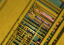
Synthetic detail of a micromanufactured integrated circuit through four layers of planarized copper interconnect, down to the polysilicon (pink), wells (greyish) and substrate (green)
679:
mixture (a.k.a. Piranha) removes organics. Hydrogen fluoride removes native oxide from silicon surface. These are all wet cleaning steps in solutions. Dry cleaning methods include
695:. Pre-gate cleaning is the most critical cleaning step in CMOS fabrication: it ensures that the ca. 2 nm thick oxide of a MOS transistor can be grown in an orderly fashion.
772:
Löper, Philipp; Stuckelberger, Michael; Niesen, Bjoern; Werner, Jérémie; Filipič, Miha; Moon, Soo-Jin; Yum, Jun-Ho; Topič, Marko; De Wolf, Stefaan; Ballif, Christophe (2015).
591:
a wide variety of other processes for cleaning, planarizing, or modifying the chemical properties of microfabricated devices can also be performed. Some examples include:
1022:
1652:
289:
Microfabrication is actually a collection of technologies which are utilized in making microdevices. Some of them have very old origins, not connected to
332:
To fabricate a microdevice, many processes must be performed, one after the other, many times repeatedly. These processes typically include depositing a
1810:
1499:
1724:
474:
1471:
1441:
1375:
1281:
1254:
1227:
1208:
1077:
245:
fabrication and integrated circuit technology are terms used instead of microfabrication, but microfabrication is the broad general term.
1729:
1657:
155:
774:"Complex Refractive Index Spectra of CH3NH3PbI3 Perovskite Thin Films Determined by Spectroscopic Ellipsometry and Spectrophotometry"
1412:
1348:
1329:
1300:
1181:
1154:
1127:
1106:
945:
861:
760:
608:
306:
65:(Japanese terminology) and their subfields have re-used, adapted or extended microfabrication methods. These subfields include
699:, and all high temperature steps are very sensitive to contamination, and cleaning steps must precede high temperature steps.
1714:
1555:
1519:
554:
242:
151:
58:
718:: first they remove all unwanted bits and pieces, and then they reconstruct the desired pattern so that the game can go on.
1719:
1492:
376:
layers that constitute the final device. Modern microprocessors are made with 30 masks while a few masks suffice for a
145:
54:
557:(MEMS) "parts or structures with at least two dimensions in the submillimeter range." It includes techniques such as
1770:
1626:
537:
512:
396:
Microfabricated devices are not generally freestanding devices but are usually formed over or in a thicker support
337:
938:
Micro-scaled
Products Development via Microforming: Deformation Behaviours, Processes, Tooling and its Realization
1461:
737:
566:
531:
458:
435:
326:
238:
1820:
1760:
1485:
914:
368:
steps, and many others are performed. The complexity of microfabrication processes can be described by their
1815:
1545:
659:
Cleanrooms provide passive cleanliness but the wafers are also actively cleaned before every critical step.
562:
322:
1704:
1672:
1603:
595:
469:
365:
93:
1017:
1012:
1608:
656:
are micrometers in size, and their presence will destroy the functionality of a microfabricated device.
1780:
527:
418:
184:
124:
1739:
1709:
727:
599:
397:
234:
161:
141:
981:
464:
353:
310:
278:
176:
72:
Miniaturization of various devices presents challenges in many areas of science and engineering:
50:
201:
1319:
1117:
1437:
1408:
1381:
1371:
1354:
1344:
1325:
1306:
1296:
1277:
1260:
1250:
1233:
1223:
1204:
1177:
1150:
1123:
1102:
1073:
1032:
1006:
941:
857:
849:
793:
756:
668:
425:
385:
274:
81:
30:
1088:
1775:
1647:
1429:
1423:
1400:
1394:
1196:
1169:
1142:
1094:
1065:
1059:
973:
893:
825:
785:
704:
603:
497:
357:
218:
89:
85:
964:
Fu, M.W.; Chan, W.L. (2013). "A review on the state-of-the-art microforming technologies".
1524:
1508:
1465:
732:
115:
820:
Engel, U.; Eckstein, R. (2002). "Microforming - From Basic research to its realization".
569:, forming system stability, mechanical properties, and other size-related effects on the
49:
scales and smaller. Historically, the earliest microfabrication processes were used for
1662:
1631:
1580:
1529:
653:
578:
558:
523:
493:
portions of the film which will be removed. Examples of patterning techniques include:
314:
62:
829:
755:
Nitaigour
Premchand Mahalik (2006) "Micromanufacturing and Nanotechnology", Springer,
1804:
985:
715:
672:
401:
388:
photography, with many patterns aligned to each other to create the final structure.
377:
290:
66:
42:
1027:
237:
are in use. Micromachining, semiconductor processing, microelectronic fabrication,
1734:
1046:: Microelectronics and Nanometer Structures: Processing, Measurement, and Phenomena
617:
318:
105:
667:-peroxide solution removes organic contamination and particles; RCA-2 cleaning in
17:
898:
277:
techniques which have successfully been applied in the microregime. For example,
633:
570:
550:
381:
294:
1677:
1598:
1550:
1368:
Ultraclean
Surface Processing of Silicon Wafers: Secrets of VLSI Manufacturing
1200:
1146:
977:
261:
195:
171:
97:
46:
1459:
Videos and animations on microfabrication techniques and related applications
1385:
1237:
1785:
1358:
1310:
1264:
696:
660:
629:
414:
333:
302:
205:
191:
109:
77:
797:
714:
Wafer cleaning and surface preparation work similarly to the machines in a
1433:
1173:
1098:
1069:
881:
1667:
1590:
688:
676:
649:
637:
266:
230:
336:, patterning the film with the desired micro features, and removing (or
1404:
708:
692:
664:
481:
373:
298:
281:
of DVDs involves fabrication of submicrometer-sized spots on the disc.
270:
222:
165:
101:
73:
1458:
789:
711:
from wafer boxes, and this might be different depending on wait time.
640:, vibrations and electrical disturbances are under stringent control.
1618:
1572:
882:"A review on micro-manufacturing, micro-forming and their key issues"
680:
773:
413:
Microfabricated devices are typically constructed using one or more
1324:. Silicon Processing for the VLSI Era. Vol. 1. Lattice Press.
1755:
1477:
936:
Fu, M.W.; Chan, W.L. (2014). "Chapter 4: Microforming
Processes".
684:
641:
451:
446:
441:
430:
361:
226:
180:
114:
57:" or "semiconductor device fabrication". In the last two decades,
29:
400:. For electronic applications, semiconducting substrates such as
1765:
645:
1481:
1043:
1037:
614:
Wafer cleaning, also known as "surface preparation" (see below)
632:, where air has been filtered of particle contamination and
691:
bake at elevated temperature to remove native oxide before
1422:
Meyrueis, P.; Sakoda, K.; Van de Voorde, M., eds. (2017).
1341:
The
Science and Engineering of Microelectronic Fabrication
966:
International
Journal of Advanced Manufacturing Technology
940:. Springer Science & Business Media. pp. 73–130.
915:"Process Analysis and Variation Control in Micro-stamping"
687:
plasma treatments to remove unwanted surface layers, or
577:
In microforming, the ratio of the total surface area of
913:
317:
is also a 19th-century technique adapted to produce
1748:
1697:
1690:
1640:
1617:
1589:
1571:
1564:
1538:
1393:Geschke, O.; Klank, H.; Telleman, P., eds. (2004).
1276:(6th ed.). McGraw-Hill. p. 1302905242.
1218:Plummer, J.D.; Deal, M.D.; Griffin, P.B. (2012).
405:separated devices toward the end of fabrication.
352:), for suitable device behavior. For example, in
217:Microfabrication technologies originate from the
1396:Microsystem Engineering of Lab-on-a-chip Devices
671:-peroxide mixture removes metallic impurities.
1653:Radio-frequency microelectromechanical systems
1191:Widmann, D.; Mader, H.; Friedrich, H. (2000).
1023:Journal of Micromechanics and Microengineering
875:
873:
843:
841:
839:
815:
813:
549:Microforming is a microfabrication process of
309:, and many of the vacuum techniques come from
221:industry, and the devices are usually made on
1493:
8:
27:Fabrication at micrometre scales and smaller
1293:Introduction to Microelectronic Fabrication
1694:
1568:
1500:
1486:
1478:
1044:Journal of Vacuum Science and Technology B
1038:Journal of Vacuum Science and Technology A
959:
957:
822:Journal of Materials Processing Technology
1668:Biological microelectromechanical systems
1343:(2nd ed.). Oxford University Press.
1007:Journal of Microelectromechanical Systems
897:
778:The Journal of Physical Chemistry Letters
248:Traditional machining techniques such as
1247:Fundamentals of Semiconductor Processing
123:
748:
61:(MEMS), microsystems (European usage),
1166:Micromanufacturing and Nanotechnology
1033:IEEE Transactions of Electron Devices
7:
1425:Micro- and Nanophotonic Technologies
1119:Micromachined Transducers Sourcebook
628:Microfabrication is carried out in
1658:Microoptoelectromechanical systems
573:(grain) structure and boundaries:
372:. This is the number of different
156:microoptoelectromechanical systems
25:
1193:Technology of Integrated Circuits
1018:Sensors and Actuators B: Chemical
1013:Sensors and Actuators A: Physical
609:Chemical-mechanical planarization
321:scale structures, as are various
137:Microfabricated devices include:
1811:Semiconductor device fabrication
1137:Brodie, I.; Muray, J.J. (1982).
1090:Fundamentals of Microfabrication
1061:Introduction to Microfabrication
624:Cleanliness in wafer fabrication
1318:Wolf, S.; Tauber, R.N. (2000).
1295:(2nd ed.). Prentice Hall.
1222:(2nd ed.). Prentice Hall.
1139:The Physics of Microfabrication
856:. CRC Press. pp. 263–282.
1520:Microelectromechanical systems
880:Razali, A.R.; Qin, Y. (2013).
356:fabrication there are some 30
348:) and extinction coefficient (
208:, energy harvesters/scavengers
152:microelectromechanical systems
59:microelectromechanical systems
1:
1472:MicroManufacturing Conference
1245:May, G.S.; Sze, S.S. (2004).
848:Dixit, U.S.; Das, R. (2012).
830:10.1016/S0924-0136(02)00415-6
707:), or they may have gathered
555:microelectromechanical system
384:. Microfabrication resembles
311:19th century physics research
899:10.1016/j.proeng.2013.02.086
854:Micromanufacturing Processes
850:"Chapter 15: Microextrusion"
567:deformation load and defects
364:steps, 20 etching steps, 10
53:fabrication, also known as "
1093:(2nd ed.). CRC Press.
250:electro-discharge machining
146:semiconductor manufacturing
55:semiconductor manufacturing
1837:
1627:Digital micromirror device
513:Etching (microfabrication)
510:
431:Local oxidation of silicon
260:have been scaled from the
1515:
1201:10.1007/978-3-662-04160-4
1147:10.1007/978-1-4899-2160-4
1040:: Vacuum, Surfaces, Films
978:10.1007/s00170-012-4661-7
917:. Northwestern University
824:. 125–126 (2002): 35–44.
738:Semiconductor fabrication
532:deep reactive-ion etching
459:Physical vapor deposition
436:Chemical vapor deposition
239:semiconductor fabrication
1761:Shallow trench isolation
190:sensors (microsensors) (
45:miniature structures of
1546:Interdigital transducer
1339:Campbell, S.A. (2001).
1220:Silicon VLSI Technology
1116:Kovacs, G.T.A. (1998).
1064:(2nd ed.). Wiley.
852:. In Jain, V.K. (ed.).
254:spark erosion machining
128:Detail of an etch step.
1705:Surface micromachining
1604:Scratch drive actuator
1164:Mahalik, N.P. (2006).
1058:Franssila, S. (2010).
703:energetic ions during
584:
470:Evaporative deposition
129:
121:
35:
1434:10.1002/9783527800728
1291:Jaeger, R.C. (2002).
1274:Microchip Fabrication
1272:van Zant, P. (2014).
1174:10.1007/3-540-29339-6
1099:10.1201/9781482274004
1070:10.1002/9781119990413
575:
344:), refractive index (
185:thin-film transistors
127:
118:
33:
1781:Silicon on insulator
1366:Hattori, T. (2011).
1087:Madou, M.J. (2002).
886:Procedia Engineering
528:reactive-ion etching
419:Thin film deposition
409:Deposition or growth
307:optics manufacturing
162:microfluidic devices
144:(“microchips”) (see
1740:3D microfabrication
1710:Bulk micromachining
728:3D microfabrication
540:or chemical etching
225:wafers even though
177:flat panel displays
142:integrated circuits
1715:HAR micromachining
1464:2022-02-06 at the
1405:10.1002/3527601651
1321:Process technology
305:was borrowed from
279:injection moulding
130:
122:
51:integrated circuit
41:is the process of
36:
18:Micromanufacturing
1798:
1797:
1794:
1793:
1686:
1685:
1443:978-3-527-34037-8
1377:978-3-642-08272-6
1283:978-0-07-182101-8
1256:978-0-471-23279-7
1229:978-0-13-614156-3
1210:978-3-662-04160-4
1079:978-1-119-99041-3
892:(2013): 665–672.
790:10.1021/jz502471h
669:hydrogen chloride
600:thermal diffusion
475:Electron beam PVD
426:Thermal oxidation
386:multiple exposure
82:materials science
16:(Redirected from
1828:
1776:Photolithography
1695:
1648:Millipede memory
1609:Thermal actuator
1569:
1539:Basic structures
1502:
1495:
1488:
1479:
1447:
1418:
1389:
1362:
1335:
1314:
1287:
1268:
1241:
1214:
1187:
1160:
1141:. Plenum Press.
1133:
1112:
1083:
990:
989:
972:(9): 2411–2437.
961:
952:
951:
933:
927:
926:
924:
922:
910:
904:
903:
901:
877:
868:
867:
845:
834:
833:
817:
808:
807:
805:
804:
769:
763:
753:
705:ion implantation
604:ion implantation
579:grain boundaries
498:Photolithography
219:microelectronics
90:microlithography
86:computer science
39:Microfabrication
21:
1836:
1835:
1831:
1830:
1829:
1827:
1826:
1825:
1821:Microtechnology
1801:
1800:
1799:
1790:
1744:
1682:
1636:
1613:
1585:
1560:
1534:
1525:Microtechnology
1511:
1509:Microtechnology
1506:
1466:Wayback Machine
1455:
1450:
1444:
1421:
1415:
1392:
1378:
1365:
1351:
1338:
1332:
1317:
1303:
1290:
1284:
1271:
1257:
1244:
1230:
1217:
1211:
1190:
1184:
1163:
1157:
1136:
1130:
1122:. McGraw-Hill.
1115:
1109:
1086:
1080:
1057:
998:
996:Further reading
993:
963:
962:
955:
948:
935:
934:
930:
920:
918:
912:
911:
907:
879:
878:
871:
864:
847:
846:
837:
819:
818:
811:
802:
800:
771:
770:
766:
754:
750:
746:
733:Nanofabrication
724:
626:
589:
547:
515:
509:
490:
411:
394:
287:
233:and many other
215:
135:
28:
23:
22:
15:
12:
11:
5:
1834:
1832:
1824:
1823:
1818:
1816:Nanotechnology
1813:
1803:
1802:
1796:
1795:
1792:
1791:
1789:
1788:
1783:
1778:
1773:
1768:
1763:
1758:
1752:
1750:
1746:
1745:
1743:
1742:
1737:
1732:
1727:
1722:
1717:
1712:
1707:
1701:
1699:
1692:
1688:
1687:
1684:
1683:
1681:
1680:
1675:
1670:
1665:
1663:Microphotonics
1660:
1655:
1650:
1644:
1642:
1638:
1637:
1635:
1634:
1632:Optical switch
1629:
1623:
1621:
1615:
1614:
1612:
1611:
1606:
1601:
1595:
1593:
1587:
1586:
1584:
1583:
1581:Microbolometer
1577:
1575:
1566:
1562:
1561:
1559:
1558:
1553:
1548:
1542:
1540:
1536:
1535:
1533:
1532:
1530:Micromachinery
1527:
1522:
1516:
1513:
1512:
1507:
1505:
1504:
1497:
1490:
1482:
1476:
1475:
1469:
1454:
1453:External links
1451:
1449:
1448:
1442:
1419:
1413:
1390:
1376:
1363:
1349:
1336:
1330:
1315:
1301:
1288:
1282:
1269:
1255:
1242:
1228:
1215:
1209:
1188:
1182:
1161:
1155:
1134:
1128:
1113:
1107:
1084:
1078:
1054:
1048:
1047:
1041:
1035:
1030:
1025:
1020:
1015:
1010:
997:
994:
992:
991:
953:
946:
928:
905:
869:
862:
835:
809:
764:
747:
745:
742:
741:
740:
735:
730:
723:
720:
625:
622:
621:
620:
615:
612:
606:
588:
585:
559:microextrusion
546:
543:
542:
541:
535:
524:plasma etching
511:Main article:
508:
505:
504:
503:
502:Shadow masking
500:
489:
486:
485:
484:
479:
478:
477:
472:
467:
456:
455:
454:
449:
444:
433:
428:
410:
407:
402:silicon wafers
393:
390:
315:Electroplating
286:
283:
258:laser drilling
214:
211:
210:
209:
199:
188:
174:
169:
159:
149:
134:
131:
26:
24:
14:
13:
10:
9:
6:
4:
3:
2:
1833:
1822:
1819:
1817:
1814:
1812:
1809:
1808:
1806:
1787:
1784:
1782:
1779:
1777:
1774:
1772:
1769:
1767:
1764:
1762:
1759:
1757:
1754:
1753:
1751:
1747:
1741:
1738:
1736:
1733:
1731:
1728:
1726:
1723:
1721:
1718:
1716:
1713:
1711:
1708:
1706:
1703:
1702:
1700:
1696:
1693:
1689:
1679:
1676:
1674:
1673:Microfluidics
1671:
1669:
1666:
1664:
1661:
1659:
1656:
1654:
1651:
1649:
1646:
1645:
1643:
1639:
1633:
1630:
1628:
1625:
1624:
1622:
1620:
1616:
1610:
1607:
1605:
1602:
1600:
1597:
1596:
1594:
1592:
1588:
1582:
1579:
1578:
1576:
1574:
1570:
1567:
1563:
1557:
1554:
1552:
1549:
1547:
1544:
1543:
1541:
1537:
1531:
1528:
1526:
1523:
1521:
1518:
1517:
1514:
1510:
1503:
1498:
1496:
1491:
1489:
1484:
1483:
1480:
1473:
1470:
1467:
1463:
1460:
1457:
1456:
1452:
1445:
1439:
1435:
1431:
1427:
1426:
1420:
1416:
1414:3-527-30733-8
1410:
1406:
1402:
1398:
1397:
1391:
1387:
1383:
1379:
1373:
1369:
1364:
1360:
1356:
1352:
1350:0-19-513605-5
1346:
1342:
1337:
1333:
1331:0-9616721-6-1
1327:
1323:
1322:
1316:
1312:
1308:
1304:
1302:0-201-44494-1
1298:
1294:
1289:
1285:
1279:
1275:
1270:
1266:
1262:
1258:
1252:
1248:
1243:
1239:
1235:
1231:
1225:
1221:
1216:
1212:
1206:
1202:
1198:
1194:
1189:
1185:
1183:3-540-25377-7
1179:
1175:
1171:
1167:
1162:
1158:
1156:1-4899-2160-5
1152:
1148:
1144:
1140:
1135:
1131:
1129:0-07-290722-3
1125:
1121:
1120:
1114:
1110:
1108:0-8493-0826-7
1104:
1100:
1096:
1092:
1091:
1085:
1081:
1075:
1071:
1067:
1063:
1062:
1056:
1055:
1053:
1052:
1045:
1042:
1039:
1036:
1034:
1031:
1029:
1028:Lab on a Chip
1026:
1024:
1021:
1019:
1016:
1014:
1011:
1008:
1005:
1004:
1003:
1002:
995:
987:
983:
979:
975:
971:
967:
960:
958:
954:
949:
947:9781447163268
943:
939:
932:
929:
916:
909:
906:
900:
895:
891:
887:
883:
876:
874:
870:
865:
863:9781439852903
859:
855:
851:
844:
842:
840:
836:
831:
827:
823:
816:
814:
810:
799:
795:
791:
787:
783:
779:
775:
768:
765:
762:
761:3-540-25377-7
758:
752:
749:
743:
739:
736:
734:
731:
729:
726:
725:
721:
719:
717:
716:bowling alley
712:
710:
706:
700:
698:
694:
690:
686:
682:
678:
674:
673:Sulfuric acid
670:
666:
662:
657:
655:
651:
647:
643:
639:
635:
631:
623:
619:
616:
613:
610:
607:
605:
601:
597:
594:
593:
592:
586:
583:
580:
574:
572:
568:
564:
563:microstamping
560:
556:
552:
544:
539:
536:
533:
529:
525:
522:Dry etching (
521:
520:
519:
514:
506:
501:
499:
496:
495:
494:
487:
483:
480:
476:
473:
471:
468:
466:
463:
462:
460:
457:
453:
450:
448:
445:
443:
440:
439:
437:
434:
432:
429:
427:
424:
423:
422:
420:
416:
408:
406:
403:
399:
391:
389:
387:
383:
379:
375:
371:
367:
363:
359:
355:
351:
347:
343:
339:
335:
330:
328:
324:
320:
316:
312:
308:
304:
300:
296:
292:
291:manufacturing
284:
282:
280:
276:
272:
268:
263:
259:
255:
251:
246:
244:
240:
236:
232:
228:
224:
220:
212:
207:
203:
200:
197:
193:
189:
186:
182:
178:
175:
173:
170:
167:
163:
160:
157:
153:
150:
147:
143:
140:
139:
138:
133:Fields of use
132:
126:
117:
113:
111:
107:
103:
99:
95:
91:
87:
83:
79:
75:
70:
68:
67:microfluidics
64:
63:micromachines
60:
56:
52:
48:
44:
40:
32:
19:
1735:Wire bonding
1565:Applications
1556:Microchannel
1424:
1395:
1370:. Springer.
1367:
1340:
1320:
1292:
1273:
1246:
1219:
1195:. Springer.
1192:
1168:. Springer.
1165:
1138:
1118:
1089:
1060:
1050:
1049:
1000:
999:
969:
965:
937:
931:
919:. Retrieved
908:
889:
885:
853:
821:
801:. Retrieved
784:(1): 66–71.
781:
777:
767:
751:
713:
701:
658:
627:
618:Wire bonding
590:
576:
548:
545:Microforming
516:
491:
412:
395:
380:device or a
378:microfluidic
369:
349:
345:
341:
331:
329:techniques.
288:
257:
253:
249:
247:
216:
168:print heads)
136:
71:
38:
37:
1725:Lithography
661:RCA-1 clean
634:temperature
571:crystallite
551:microsystem
538:Wet etching
382:laser diode
358:lithography
354:memory chip
295:lithography
196:nanosensors
172:solar cells
154:(MEMS) and
120:same plane.
43:fabricating
1805:Categories
1720:Deposition
1678:Micropower
1599:Comb drive
1551:Cantilever
803:2021-11-16
744:References
630:cleanrooms
598:by either
526:) such as
488:Patterning
465:Sputtering
415:thin films
392:Substrates
370:mask count
360:steps, 10
319:micrometre
262:millimeter
206:fuel cells
202:power MEMS
192:biosensors
98:thin films
47:micrometre
1786:Smart cut
1691:Processes
1591:Actuators
1428:. Wiley.
1399:. Wiley.
1386:751530070
1249:. Wiley.
1238:753300108
986:110879846
697:Oxidation
530:(RIE) or
398:substrate
362:oxidation
327:embossing
303:Polishing
285:Processes
235:substrate
110:polishing
78:chemistry
1771:Lift-off
1749:Specific
1619:Switches
1462:Archived
1359:45209102
1311:48226051
1265:52333554
1009:(J.MEMS)
1001:Journals
921:18 March
798:26263093
722:See also
709:polymers
689:hydrogen
677:peroxide
650:bacteria
638:humidity
323:stamping
275:moulding
231:plastics
1730:Etching
1698:General
1573:Sensors
693:epitaxy
665:ammonia
507:Etching
482:Epitaxy
374:pattern
338:etching
299:etching
293:, like
271:casting
267:imprint
256:, and
223:silicon
213:Origins
166:ink jet
158:(MOEMS)
106:bonding
102:etching
74:physics
1440:
1411:
1384:
1374:
1357:
1347:
1328:
1309:
1299:
1280:
1263:
1253:
1236:
1226:
1207:
1180:
1153:
1126:
1105:
1076:
984:
944:
860:
796:
759:
681:oxygen
596:Doping
534:(DRIE)
461:(PVD)
438:(CVD)
366:doping
108:, and
94:doping
1756:LOCOS
1641:Other
1051:Books
982:S2CID
685:argon
654:cells
642:Smoke
611:(CMP)
587:Other
452:PECVD
447:LPCVD
442:APCVD
417:(see
227:glass
181:AMLCD
179:(see
1766:LIGA
1438:ISBN
1409:ISBN
1382:OCLC
1372:ISBN
1355:OCLC
1345:ISBN
1326:ISBN
1307:OCLC
1297:ISBN
1278:ISBN
1261:OCLC
1251:ISBN
1234:OCLC
1224:ISBN
1205:ISBN
1178:ISBN
1151:ISBN
1124:ISBN
1103:ISBN
1074:ISBN
942:ISBN
923:2016
858:ISBN
794:PMID
757:ISBN
683:and
652:and
646:dust
334:film
325:and
273:and
243:MEMS
183:and
1430:doi
1401:doi
1197:doi
1170:doi
1143:doi
1095:doi
1066:doi
974:doi
894:doi
826:doi
786:doi
663:in
602:or
553:or
297:or
104:,
100:,
1807::
1436:.
1407:.
1380:.
1353:.
1305:.
1259:.
1232:.
1203:.
1176:.
1149:.
1101:.
1072:.
980:.
970:67
968:.
956:^
890:53
888:.
884:.
872:^
838:^
812:^
792:.
780:.
776:.
648:,
644:,
636:,
561:,
313:.
301:.
269:,
252:,
241:,
229:,
204:,
194:,
112:.
96:,
92:,
84:,
80:,
76:,
1501:e
1494:t
1487:v
1474:.
1468:.
1446:.
1432::
1417:.
1403::
1388:.
1361:.
1334:.
1313:.
1286:.
1267:.
1240:.
1213:.
1199::
1186:.
1172::
1159:.
1145::
1132:.
1111:.
1097::
1082:.
1068::
988:.
976::
950:.
925:.
902:.
896::
866:.
832:.
828::
806:.
788::
782:6
675:-
350:k
346:n
342:t
198:)
187:)
164:(
148:)
20:)
Text is available under the Creative Commons Attribution-ShareAlike License. Additional terms may apply.