1138:
1146:
1054:
is to provide a carbon source, the role of hydrogen is to provide H atoms to corrode amorphous C, and improve the quality of graphene. But excessive H atoms can also corrode graphene. As a result, the integrity of the crystal lattice is destroyed, and the quality of graphene is deteriorated. Therefore, by optimizing the flow rate of methane and hydrogen gases in the growth process, the quality of graphene can be improved.
216:
224:
410:(LCVD) - This CVD process uses lasers to heat spots or lines on a substrate in semiconductor applications. In MEMS and in fiber production the lasers are used rapidly to break down the precursor gas—process temperature can exceed 2000 °C—to build up a solid structure in much the same way as laser sintering based 3-D printers build up solids from powders.
1129:
things down, graphene nanoribbons of less than 10 nm in width do exhibit electronic bandgaps and are therefore potential candidates for digital devices. Precise control over their dimensions, and hence electronic properties, however, represents a challenging goal, and the ribbons typically possess rough edges that are detrimental to their performance.
38:
1176:) and involves feeding varying amounts of gases into a chamber, energizing them and providing conditions for diamond growth on the substrate. The gases always include a carbon source, and typically include hydrogen as well, though the amounts used vary greatly depending on the type of diamond being grown. Energy sources include
1120:
vertical cold wall system utilizing resistive heating by passing direct current through the substrate. It provided conclusive insight into a typical surface-mediated nucleation and growth mechanism involved in two-dimensional materials grown using catalytic CVD under conditions sought out in the semiconductor industry.
1199:
of any bulk material, layering diamond onto high heat-producing electronics (such as optics and transistors) allows the diamond to be used as a heat sink. Diamond films are being grown on valve rings, cutting tools, and other objects that benefit from diamond's hardness and exceedingly low wear rate.
1163:
by creating the circumstances necessary for carbon atoms in a gas to settle on a substrate in crystalline form. CVD of diamonds has received much attention in the materials sciences because it allows many new applications that had previously been considered too expensive. CVD diamond growth typically
1128:
In spite of graphene's exciting electronic and thermal properties, it is unsuitable as a transistor for future digital devices, due to the absence of a bandgap between the conduction and valence bands. This makes it impossible to switch between on and off states with respect to electron flow. Scaling
288:
Direct liquid injection CVD (DLICVD) – CVD in which the precursors are in liquid form (liquid or solid dissolved in a convenient solvent). Liquid solutions are injected in a vaporization chamber towards injectors (typically car injectors). The precursor vapors are then transported to the substrate as
1227:
carbon, and there are many different types of diamond included in this. By regulating the processing parameters—especially the gases introduced, but also including the pressure the system is operated under, the temperature of the diamond, and the method of generating plasma—many different materials
1066:
The direct growth of high-quality, large single-crystalline domains of graphene on a dielectric substrate is of vital importance for applications in electronics and optoelectronics. Combining the advantages of both catalytic CVD and the ultra-flat dielectric substrate, gaseous catalyst-assisted CVD
1053:
Although methane is the most popular carbon source, hydrogen is required during the preparation process to promote carbon deposition on the substrate. If the flow ratio of methane and hydrogen are not appropriate, it will cause undesirable results. During the growth of graphene, the role of methane
1119:
Cold wall CVD technique can be used to study the underlying surface science involved in graphene nucleation and growth as it allows unprecedented control of process parameters like gas flow rates, temperature and pressure as demonstrated in a recent study. The study was carried out in a home-built
744:
Lower temperature deposition of silicon dioxide and doped glasses from TEOS using ozone rather than oxygen has also been explored (350 to 500 °C). Ozone glasses have excellent conformality but tend to be hygroscopic – that is, they absorb water from the air due to the incorporation of silanol
368:
Hot filament CVD (HFCVD) – also known as catalytic CVD (Cat-CVD) or more commonly, initiated CVD, this process uses a hot filament to chemically decompose the source gases. The filament temperature and substrate temperature thus are independently controlled, allowing colder temperatures for better
1191:
Using CVD, films of diamond can be grown over large areas of substrate with control over the properties of the diamond produced. In the past, when high pressure high temperature (HPHT) techniques were used to produce a diamond, the result was typically very small free-standing diamonds of varying
323:
to enhance chemical reaction rates of the precursors. PECVD processing allows deposition at lower temperatures, which is often critical in the manufacture of semiconductors. The lower temperatures also allow for the deposition of organic coatings, such as plasma polymers, that have been used for
2837:
from
Electronic Materials and Processing: Proceedings of the First Electronic Materials and Processing Congress held in conjunction with the 1988 World Materials Congress Chicago, Illinois, USA, 24–30 September 1988, Edited by Prabjit Singh (Sponsored by the Electronic Materials and Processing
1062:
The use of catalyst is viable in changing the physical process of graphene production. Notable examples include iron nanoparticles, nickel foam, and gallium vapor. These catalysts can either be used in situ during graphene buildup, or situated at some distance away at the deposition area. Some
727:
containing both boron and phosphorus (borophosphosilicate glass, BPSG) undergo viscous flow at lower temperatures; around 850 °C is achievable with glasses containing around 5 weight % of both constituents, but stability in air can be difficult to achieve. Phosphorus oxide in high
697:("P-glass") can be used to smooth out uneven surfaces. P-glass softens and reflows at temperatures above 1000 °C. This process requires a phosphorus concentration of at least 6%, but concentrations above 8% can corrode aluminium. Phosphorus is deposited from phosphine gas and oxygen:
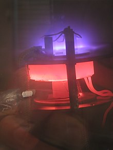
1188:, among others. The energy source is intended to generate a plasma in which the gases are broken down and more complex chemistries occur. The actual chemical process for diamond growth is still under study and is complicated by the very wide variety of diamond growth processes used.
1801:
1192:
sizes. With CVD diamond, growth areas of greater than fifteen centimeters (six inches) in diameter have been achieved, and much larger areas are likely to be successfully coated with diamond in the future. Improving this process is key to enabling several important applications.
1112:
Raman spectroscopy is used to characterize and identify the graphene particles; X-ray spectroscopy is used to characterize chemical states; TEM is used to provide fine details regarding the internal composition of graphene; SEM is used to examine the surface and topography.
2282:
Murakami, Katsuhisa; Tanaka, Shunsuke; Hirukawa, Ayaka; Hiyama, Takaki; Kuwajima, Tomoya; Kano, Emi; Takeguchi, Masaki; Fujita, Jun-ichi (2015). "Direct synthesis of large area graphene on insulating substrate by gallium vapor-assisted chemical vapor deposition".
1699:
Cruz, A.; Stassen, I.; Krishtab, M.; Marcoen, K.; Stassin, T.; Rodríguez-Hermida, S.; Teyssandier, J.; Pletincx, S.; Verbeke, R.; Rubio-Giménez, V.; Tatay, S.; Martí-Gastaldo, C.; Meersschaut, J.; Vereecken, P. M.; De Feyter, S.; Hauffman, T.; Ameloot, R. (2019).
1100:
Standard quartz tubing and chambers are used in CVD of graphene. Quartz is chosen because it has a very high melting point and is chemically inert. In other words, quartz does not interfere with any physical or chemical reactions regardless of the conditions.
440:
confer wear-resistance. Polymerization by CVD, perhaps the most versatile of all applications, allows for super-thin coatings which possess some very desirable qualities, such as lubricity, hydrophobicity and weather-resistance to name a few. The CVD of
403:
Photo-initiated CVD (PICVD) – This process uses UV light to stimulate chemical reactions. It is similar to plasma processing, given that plasmas are strong emitters of UV radiation. Under certain conditions, PICVD can be operated at or near atmospheric
1082:
On the other hand, temperatures used range from 800 to 1050 °C. High temperatures translate to an increase of the rate of reaction. Caution has to be exercised as high temperatures do pose higher danger levels in addition to greater energy costs.
392:
Rapid thermal CVD (RTCVD) – This CVD process uses heating lamps or other methods to rapidly heat the wafer substrate. Heating only the substrate rather than the gas or chamber walls helps reduce unwanted gas-phase reactions that can lead to
1078:
Most systems use LPCVD with pressures ranging from 1 to 1500 Pa. However, some still use APCVD. Low pressures are used more commonly as they help prevent unwanted reactions and produce more uniform thickness of deposition on the substrate.
1752:
445:, a class of crystalline nanoporous materials, has recently been demonstrated. Recently scaled up as an integrated cleanroom process depositing large-area substrates, the applications for these films are anticipated in gas sensing and
947:
when deposited onto silicon. Mo, Ta and Ti are deposited by LPCVD, from their pentachlorides. Nickel, molybdenum, and tungsten can be deposited at low temperatures from their carbonyl precursors. In general, for an arbitrary metal
2045:
Liu, Zhuchen; Tu, Zhiqiang; Li, Yongfeng; Yang, Fan; Han, Shuang; Yang, Wang; Zhang, Liqiang; Wang, Gang; Xu, Chunming (2014-05-01). "Synthesis of three-dimensional graphene from petroleum asphalt by chemical vapor deposition".
1244:
can be grown. Some polycrystalline diamond grains are surrounded by thin, non-diamond carbon, while others are not. These different factors affect the diamond's hardness, smoothness, conductivity, optical properties and more.
732:
can also precipitate from the flowing glass on cooling; these crystals are not readily etched in the standard reactive plasmas used to pattern oxides, and will result in circuit defects in integrated circuit manufacturing.
331:
Remote plasma-enhanced CVD (RPECVD) – Similar to PECVD except that the wafer substrate is not directly in the plasma discharge region. Removing the wafer from the plasma region allows processing temperatures down to room
449:. CVD techniques are advantageous for membrane coatings as well, such as those in desalination or water treatment, as these coatings can be sufficiently uniform (conformal) and thin that they do not clog membrane pores.
1091:
Hydrogen gas and inert gases such as argon are flowed into the system. These gases act as a carrier, enhancing surface reaction and improving reaction rate, thereby increasing deposition of graphene onto the substrate.
284:
Aerosol assisted CVD (AACVD) – CVD in which the precursors are transported to the substrate by means of a liquid/gas aerosol, which can be generated ultrasonically. This technique is suitable for use with non-volatile
300:
Cold wall CVD – CVD in which only the substrate is directly heated either by induction or by passing current through the substrate itself or a heater in contact with the substrate. The chamber walls are at room
2126:
Wei, Dacheng; Lu, Yunhao; Han, Cheng; Niu, Tianchao; Chen, Wei; Wee, Andrew Thye Shen (2013-10-31). "Critical
Crystal Growth of Graphene on Dielectric Substrates at Low Temperature for Electronic Devices".
736:
Besides these intentional impurities, CVD oxide may contain byproducts of the deposition. TEOS produces a relatively pure oxide, whereas silane introduces hydrogen impurities, and dichlorosilane introduces
419:
CVD is commonly used to deposit conformal films and augment substrate surfaces in ways that more traditional surface modification techniques are not capable of. CVD is extremely useful in the process of
2438:
Kim, Sang-Min; Kim, Jae-Hyun; Kim, Kwang-Seop; Hwangbo, Yun; Yoon, Jong-Hyuk; Lee, Eun-Kyu; Ryu, Jaechul; Lee, Hak-Joo; Cho, Seungmin (2014). "Synthesis of CVD-graphene on rapidly heated copper foils".
1200:
In each case the diamond growth must be carefully done to achieve the necessary adhesion onto the substrate. Diamond's very high scratch resistance and thermal conductivity, combined with a lower
1050:
The most popular carbon source that is used to produce graphene is methane gas. One of the less popular choices is petroleum asphalt, notable for being inexpensive but more difficult to work with.
1316:
693:
from the oxide into adjacent layers (most notably silicon) and dope them. Oxides containing 5–15% impurities by mass are often used for this purpose. In addition, silicon dioxide alloyed with
525:-based solution. The hydrogen reduces the growth rate, but the temperature is raised to 850 or even 1050 °C to compensate. Polysilicon may be grown directly with doping, if gases such as
980:
the decomposition of metal carbonyls is often violently precipitated by moisture or air, where oxygen reacts with the metal precursor to form metal or metal oxide along with carbon dioxide.
1751:
Servi, Amelia T.; Guillen-Burrieza, Elena; Warsinger, David M.; Livernois, William; Notarangelo, Katie; Kharraz, Jehad; Lienhard V, John H.; Arafat, Hassan A.; Gleason, Karen K. (2017).
1223:
CVD growth allows one to control the properties of the diamond produced. In the area of diamond growth, the word "diamond" is used as a description of any material primarily made up of
662:
is sensitive to high temperature. Silane deposits between 300 and 500 °C, dichlorosilane at around 900 °C, and TEOS between 650 and 750 °C, resulting in a layer of
1109:
Raman spectroscopy, X-ray spectroscopy, transmission electron microscopy (TEM), and scanning electron microscopy (SEM) are used to examine and characterize the graphene samples.
2390:
Zhang, CanKun; Lin, WeiYi; Zhao, ZhiJuan; Zhuang, PingPing; Zhan, LinJie; Zhou, YingHui; Cai, WeiWei (2015-09-05). "CVD synthesis of nitrogen-doped graphene using urea".
1820:
241:
Low-pressure CVD (LPCVD) – CVD at sub-atmospheric pressures. Reduced pressures tend to reduce unwanted gas-phase reactions and improve film uniformity across the wafer.
1042:
Many variations of CVD can be utilized to synthesize graphene. Although many advancements have been made, the processes listed below are not commercially viable yet.
3428:
1514:
Gleason, Karen K.; Kenneth K.S. Lau; Jeffrey A. Caulfield (2000). "Structure and
Morphology of Fluorocarbon Films Grown by Hot Filament Chemical Vapor Deposition".
2073:
Park, Hye Jin; Meyer, Jannik; Roth, Siegmar; Skákalová, Viera (Spring 2010). "Growth and properties of few-layer graphene prepared by chemical vapor deposition".
1396:
Shareef, I. A.; Rubloff, G. W.; Anderle, M.; Gill, W. N.; Cotte, J.; Kim, D. H. (1995-07-01). "Subatmospheric chemical vapor deposition ozone/TEOS process for SiO
1286:
753:
Silicon nitride is often used as an insulator and chemical barrier in manufacturing ICs. The following two reactions deposit silicon nitride from the gas phase:
372:
3312:
1195:
The growth of diamond directly on a substrate allows the addition of many of diamond's important qualities to other materials. Since diamond has the highest
745:(Si-OH) in the glass. Infrared spectroscopy and mechanical strain as a function of temperature are valuable diagnostic tools for diagnosing such problems.
545:
Silicon dioxide (usually called simply "oxide" in the semiconductor industry) may be deposited by several different processes. Common source gases include
361:(CCVD) – Combustion Chemical Vapor Deposition or flame pyrolysis is an open-atmosphere, flame-based technique for depositing high-quality thin films and
338:(LEPECVD) - CVD employing a high density, low energy plasma to obtain epitaxial deposition of semiconductor materials at high rates and low temperatures.
3443:
1458:
Tavares, Jason; Swanson, E.J.; Coulombe, S. (2008). "Plasma
Synthesis of Coated Metal Nanoparticles with Surface Properties Tailored for Dispersion".
316:
52:
297:
Hot wall CVD – CVD in which the chamber is heated by an external power source and the substrate is heated by radiation from the heated chamber walls.
2864:
2180:"Graphene: Two-Stage Metal-Catalyst-Free Growth of High-Quality Polycrystalline Graphene Films on Silicon Nitride Substrates (Adv. Mater. 7/2013)"
1321:
1550:
382:
1487:"Hot wire CVD of heterogeneous and polycrystalline silicon semiconducting thin films for application in thin film transistors and solar cells"
862:
These films have much less tensile stress, but worse electrical properties (resistivity 10 to 10 Ω·cm, and dielectric strength 1 to 5 MV/cm).
2786:
2767:
2748:
1904:
1879:
908:, can be deposited by CVD. As of 2010, commercially cost-effective CVD for copper did not exist, although volatile sources exist, such as Cu(
1075:
Physical conditions such as surrounding pressure, temperature, carrier gas, and chamber material play a big role in production of graphene.
1497:
358:
674:. Any of these reactions may be used in LPCVD, but the silane reaction is also done in APCVD. CVD oxide invariably has lower quality than
289:
in classical CVD. This technique is suitable for use on liquid or solid precursors. High growth rates can be reached using this technique.
31:
2826:
968:
whereas the carbonyl decomposition reaction can happen spontaneously under thermal treatment or acoustic cavitation and is as follows:
3413:
1837:
1650:
Stassen, I; Styles, M; Grenci, G; Van Gorp, H; Vanderlinden, W; De Feyter, S; Falcaro, P; De Vos, D; Vereecken, P; Ameloot, R (2015).
369:
absorption rates at the substrate and higher temperatures necessary for decomposition of precursors to free radicals at the filament.
2020:
1301:
231:
CVD is practiced in a variety of formats. These processes generally differ in the means by which chemical reactions are initiated.
1201:
2626:
Sun Lee, Woong; Yu, Jin (2005). "Comparative study of thermally conductive fillers in underfill for the electronic components".
2178:
Chen, Jianyi; Guo, Yunlong; Wen, Yugeng; Huang, Liping; Xue, Yunzhou; Geng, Dechao; Wu, Bin; Luo, Birong; Yu, Gui (2013-02-14).
3337:
3133:
407:
2236:
Patel, Rajen B.; Yu, Chi; Chou, Tsengming; Iqbal, Zafar (2014). "Novel synthesis route to graphene using iron nanoparticles".
1402:
Journal of Vacuum
Science & Technology B: Microelectronics and Nanometer Structures Processing, Measurement, and Phenomena
1607:
Gleason, Karen; Ayse
Asatekin; Miles C. Barr; Samaan H. Baxamusa; Kenneth K.S. Lau; Wyatt Tenhaeff; Jingjing Xu (May 2010).
513:
This reaction is usually performed in LPCVD systems, with either pure silane feedstock, or a solution of silane with 70–80%
3453:
3433:
3249:
3226:
1968:
Maruyama, Toshiro (1994). "Electrochromic
Properties of Niobium Oxide Thin Films Prepared by Chemical Vapor Deposition".
3082:
2591:
Costello, M; Tossell, D; Reece, D; Brierley, C; Savage, J (1994). "Diamond protective coatings for optical components".
3418:
2857:
1702:"Integrated Cleanroom Process for the Vapor-Phase Deposition of Large-Area Zeolitic Imidazolate Framework Thin Films"
1551:"Photo-Initiated Chemical Vapour Deposition as a Scalable Particle Functionalization Technology (A Practical Review)"
517:. Temperatures between 600 and 650 °C and pressures between 25 and 150 Pa yield a growth rate between 10 and 20
3463:
3448:
3438:
1220:
would make it a nearly ideal non-stick coating for cookware if large substrate areas could be coated economically.
203:
1067:
paves the way for synthesizing high-quality graphene for device applications while avoiding the transfer process.
3034:
2924:
1254:
870:
Tungsten CVD, used for forming conductive contacts, vias, and plugs on a semiconductor device, is achieved from
689:"). This may have two purposes. During further process steps that occur at high temperature, the impurities may
3014:
925:
260:
2492:"Nucleation and growth of single layer graphene on electrodeposited Cu by cold wall chemical vapor deposition"
1944:
2700:
Krauss, A (2001). "Ultrananocrystalline diamond thin films for MEMS and moving mechanical assembly devices".
1116:
Sometimes, atomic force microscopy (AFM) is used to measure local properties such as friction and magnetism.
70:
method used to produce high-quality, and high-performance, solid materials. The process is often used in the
3377:
3244:
3118:
1213:
1209:
909:
574:
468:
442:
421:
2850:
1706:
1343:
1261:
of CdTe and HgTe, this material can be prepared from the dimethyl derivatives of the respective elements.
1169:
686:
97:
86:
71:
3186:
2994:
1224:
871:
537:
are added to the CVD chamber. Diborane increases the growth rate, but arsine and phosphine decrease it.
2804:
Liu T., Raabe D. and
Zaefferer S. (2008). "A 3D tomographic EBSD analysis of a CVD diamond thin film"
3342:
3216:
2964:
2954:
2814:
2709:
2674:
2635:
2600:
2554:
2503:
2448:
2399:
2341:
2292:
2245:
2191:
2136:
1977:
1753:"The effects of iCVD film thickness and conformality on the permeability and wetting of MD membranes"
1665:
1445:
Crystec
Technology Trading GmbH, Plasma Enhanced Chemical Vapor Deposition – Technology and Equipment
1409:
1196:
921:
694:
352:
183:
3289:
3148:
3009:
3362:
3284:
3206:
3181:
1281:
1137:
987:
667:
446:
171:
82:
1228:
that can be considered diamond can be made. Single-crystal diamond can be made containing various
808:
Silicon nitride deposited by LPCVD contains up to 8% hydrogen. It also experiences strong tensile
424:
at depositing extremely thin layers of material. A variety of applications for such films exist.
3269:
3191:
2939:
2929:
2570:
2527:
2472:
2415:
2331:
2261:
2108:
2082:
1793:
1733:
1531:
1364:
1311:
432:(ICs) and photovoltaic devices. Amorphous polysilicon is used in photovoltaic devices. Certain
429:
394:
143:
2545:
Das, Shantanu; Drucker, Jeff (28 May 2018). "Pre-coalescence scaling of graphene island sizes".
1486:
3423:
3382:
3347:
3317:
3274:
3211:
3196:
3108:
2999:
2782:
2763:
2744:
2519:
2464:
2367:
2320:"Silane-catalysed fast growth of large single-crystalline graphene on hexagonal boron nitride"
2209:
2160:
2152:
2100:
2016:
1900:
1875:
1833:
1785:
1681:
1425:
1306:
1233:
1160:
1154:
675:
307:
253:
159:
151:
93:
67:
3138:
3128:
3123:
2893:
2717:
2682:
2643:
2608:
2562:
2511:
2456:
2407:
2357:
2349:
2300:
2253:
2199:
2144:
2092:
2055:
2008:
1985:
1920:
1867:
1825:
1775:
1767:
1723:
1715:
1673:
1656:
1630:
1620:
1591:
1565:
1523:
1467:
1417:
1356:
1276:
983:
809:
690:
425:
320:
179:
107:
3458:
3332:
3327:
3176:
3072:
3044:
3029:
3024:
3019:
2979:
2949:
2830:
1145:
728:
concentrations interacts with ambient moisture to produce phosphoric acid. Crystals of BPO
658:
The choice of source gas depends on the thermal stability of the substrate; for instance,
472:
463:
155:
139:
135:
131:
115:
48:
3049:
17:
2795:
Okada K. (2007). "Plasma-enhanced chemical vapor deposition of nanocrystalline diamond"
2713:
2678:
2639:
2604:
2558:
2507:
2452:
2403:
2345:
2296:
2249:
2195:
2140:
1981:
1669:
1413:
816:
and dielectric strength than most insulators commonly available in microfabrication (10
3294:
3264:
3259:
2362:
2319:
1271:
917:
671:
554:
147:
111:
44:
41:
2721:
1625:
1608:
3407:
3201:
3158:
3064:
3039:
2934:
2662:
2612:
2574:
2419:
2265:
1852:
Proceedings of the Third World
Congress of Chemical Engineering, Tokyo, p. 290 (1986)
1737:
1651:
1368:
1217:
1165:
991:
678:, but thermal oxidation can only be used in the earliest stages of IC manufacturing.
566:
362:
245:
2531:
2112:
2005:
Atomic Layer Deposition of High Permittivity Oxides: Film Growth and In Situ Studies
1535:
1485:
Schropp, R.E.I.; B. Stannowski; A.M. Brockhoff; P.A.T.T. van Veenendaal; J.K. Rath.
1344:"Controlled physical properties and growth mechanism of manganese silicide nanorods"
666:(LTO). However, silane produces a lower-quality oxide than the other methods (lower
3367:
3322:
3279:
2969:
2944:
2898:
2476:
1797:
1185:
1177:
386:
376:
325:
167:
2805:
2686:
2647:
1719:
1360:
2096:
2059:
1771:
1569:
1257:
is of continuing interest for detection of infrared radiation. Consisting of an
375:(HPCVD) – This process involves both chemical decomposition of precursor gas and
3392:
3357:
3077:
2959:
2796:
1296:
1291:
813:
2823:
2515:
104:
are also produced, which are removed by gas flow through the reaction chamber.
3387:
3352:
3221:
2989:
2984:
2411:
1241:
932:
101:
100:
on the substrate surface to produce the desired deposit. Frequently, volatile
89:
2213:
2156:
2104:
1829:
1789:
1595:
1429:
244:
Ultrahigh vacuum CVD (UHVCVD) – CVD at very low pressure, typically below 10
3254:
3153:
1237:
1181:
659:
526:
518:
119:
75:
2523:
2468:
2371:
2204:
2179:
2164:
2148:
1701:
1685:
1471:
347:) – Deposits successive layers of different substances to produce layered,
215:
110:
processes widely use CVD to deposit materials in various forms, including:
1864:
Nanostructures and Nanomaterials -- Synthesis, Properties and Applications
223:
3372:
3143:
2919:
2914:
2257:
1780:
1652:"Chemical vapour deposition of zeolitic imidazolate framework thin films"
944:
940:
936:
812:, which may crack films thicker than 200 nm. However, it has higher
738:
534:
522:
514:
175:
163:
1635:
1063:
catalysts require another step to remove them from the sample material.
3092:
2842:
2460:
2353:
2012:
1728:
1382:
437:
433:
348:
335:
127:
123:
2566:
2304:
1989:
1527:
3168:
2974:
1677:
1443:
1421:
1229:
905:
550:
546:
530:
480:
259:
Sub-atmospheric CVD (SACVD) – CVD at sub-atmospheric pressures. Uses
2813:
Wild, Christoph (2008). "CVD Diamond Properties and Useful Formula"
37:
2491:
2336:
1383:"Low Pressure Chemical Vapor Deposition – Technology and Equipment"
3087:
3054:
3004:
2888:
2873:
2087:
1258:
1205:
1144:
1136:
724:
682:
344:
264:
222:
214:
36:
1945:"Chemical Vapour Deposition - an overview | ScienceDirect Topics"
1871:
1149:
Colorless gem cut from diamond grown by chemical vapor deposition
267:
to fill high aspect ratio Si structures with silicon dioxide (SiO
1173:
821:
252:). Note that in other fields, a lower division between high and
249:
2846:
238:
Atmospheric pressure CVD (APCVD) – CVD at atmospheric pressure.
817:
827:
Another two reactions may be used in plasma to deposit SiNH:
1317:
List of metal-organic chemical vapour deposition precursors
2824:
Chemical vapor deposition of dielectric and metal films
986:
layers can be produced by the thermal decomposition of
943:, nickel is widely used. These metals can form useful
2663:"Single crystal diamond for electronic applications"
336:
Low-energy plasma-enhanced chemical vapor deposition
3303:
3235:
3167:
3101:
3063:
2907:
2881:
2743:(2nd ed.). Upper Saddle River: Prentice Hall.
2318:Tang, Shujie; Wang, Haomin; Wang, Huishan (2015).
1342:
1155:Synthetic diamond § Chemical vapor deposition
952:, the chloride deposition reaction is as follows:
1609:"Designing polymer surfaces via vapor deposition"
281:Classified by physical characteristics of vapor:
2392:Science China Physics, Mechanics & Astronomy
453:Commercially important materials prepared by CVD
2739:Jaeger, Richard C. (2002). "Film Deposition".
1821:Ullmann's Encyclopedia of Industrial Chemistry
1588:Ullmann's Encyclopedia of Industrial Chemistry
1287:Electrostatic spray assisted vapour deposition
3313:Conservation and restoration of glass objects
2858:
2760:Thin-Film Deposition: Principles and Practice
1897:Semiconductor devices: physics and technology
1141:Free-standing single-crystal CVD diamond disc
8:
1866:. World Scientific Publishing. p. 248.
1818:Simmler, W. "Silicon Compounds, Inorganic".
2741:Introduction to Microelectronic Fabrication
277:Most modern CVD is either LPCVD or UHVCVD.
219:Hot-wall thermal CVD (batch operation type)
2865:
2851:
2843:
521:per minute. An alternative process uses a
2806:Sci. Technol. Adv. Mater. 9 (2008) 035013
2361:
2335:
2203:
2086:
1779:
1727:
1634:
1624:
1549:Dorval Dion, C.A.; Tavares, J.R. (2013).
681:Oxide may also be grown with impurities (
373:Hybrid physical-chemical vapor deposition
294:Classified by type of substrate heating:
53:plasma-enhanced chemical vapor deposition
2586:
2584:
2779:Principles of Chemical Vapor Deposition
1333:
1322:List of synthetic diamond manufacturers
1236:consisting of grain sizes from several
878:), which may be deposited in two ways:
385:(MOCVD) – This CVD process is based on
3429:Glass coating and surface modification
1970:Journal of the Electrochemical Society
383:Metalorganic chemical vapor deposition
85:(substrate) is exposed to one or more
2490:Das, Shantanu; Drucker, Jeff (2017).
2433:
2431:
2429:
2385:
2383:
2381:
2277:
2275:
2231:
2229:
2227:
2225:
2223:
2040:
2038:
2036:
2034:
2032:
313:Microwave plasma-assisted CVD (MPCVD)
27:Method used to apply surface coatings
7:
904:Other metals, notably aluminium and
670:, for instance), and it deposits non
359:Combustion chemical vapor deposition
235:Classified by operating conditions:
916:. Copper is typically deposited by
32:Chemical Vapor Deposition (journal)
2007:(Thesis). University of Helsinki.
1862:Cao, Guozhong; Wang, Ying (2011).
1385:. Crystec Technology Trading GmbH.
920:. Aluminium can be deposited from
487:), using the following reactions:
25:
1302:Metalorganic vapour phase epitaxy
589:). The reactions are as follows:
3444:Semiconductor device fabrication
2797:Sci. Technol. Adv. Mater. 8, 624
1807:from the original on 2018-07-23.
1503:from the original on 2005-02-15.
1202:coefficient of thermal expansion
1164:occurs under low pressure (1–27
47:(violet) enhances the growth of
30:For the scientific journal, see
3383:Radioactive waste vitrification
3338:Glass fiber reinforced concrete
2838:Division of ASM International).
1494:Materials Physics and Mechanics
1349:Journal of Alloys and Compounds
408:Laser chemical vapor deposition
1341:Sadri, Rad (15 January 2021).
1105:Methods of analysis of results
197:who intended to differentiate
1:
3250:Chemically strengthened glass
2722:10.1016/S0925-9635(01)00385-5
2702:Diamond and Related Materials
2687:10.1016/j.diamond.2003.10.017
2667:Diamond and Related Materials
2648:10.1016/j.diamond.2005.05.008
2628:Diamond and Related Materials
2593:Diamond and Related Materials
2238:Journal of Materials Research
1720:10.1021/acs.chemmater.9b03435
1626:10.1016/S1369-7021(10)70081-X
1460:Plasma Processes and Polymers
1361:10.1016/j.jallcom.2020.156693
1159:CVD can be used to produce a
51:in a laboratory-scale PECVD (
3083:Glass-ceramic-to-metal seals
2613:10.1016/0925-9635(94)90108-2
2097:10.1016/j.carbon.2009.11.030
2060:10.1016/j.matlet.2014.02.077
1899:. Wiley-India. p. 384.
1772:10.1016/j.memsci.2016.10.008
1570:10.1016/j.powtec.2013.02.024
319:(PECVD) – CVD that utilizes
1760:Journal of Membrane Science
994:according to the equation:
126:. These materials include:
3480:
2547:Journal of Applied Physics
1152:
461:
328:surface functionalization.
204:physical vapour deposition
191:chemical vapour deposition
29:
3414:Chemical vapor deposition
3114:Chemical vapor deposition
3035:Ultra low expansion glass
2925:Borophosphosilicate glass
2777:Dobkin and Zuraw (2003).
2412:10.1007/s11433-015-5717-0
1255:mercury cadmium telluride
1212:close to that of Teflon (
926:organoaluminium compounds
400:Vapor-phase epitaxy (VPE)
306:Plasma methods (see also
60:Chemical vapor deposition
18:Chemical Vapor Deposition
3353:Glass-reinforced plastic
3015:Sodium hexametaphosphate
2822:Hess, Dennis W. (1988).
2516:10.1088/1361-6528/aa593b
1830:10.1002/14356007.a24_001
1596:10.1002/14356007.a26_681
443:metal-organic frameworks
261:tetraethyl orthosilicate
3245:Anti-reflective coating
3119:Glass batch calculation
3000:Photochromic lens glass
2815:CVD Diamond Booklet PDF
2285:Applied Physics Letters
1824:. Weinheim: Wiley-VCH.
1590:, Wiley-VCH, Weinheim.
1586:(2000) "Thin Films" in
1234:Polycrystalline diamond
1214:polytetrafluoroethylene
1210:coefficient of friction
575:tetraethylorthosilicate
469:Polycrystalline silicon
422:atomic layer deposition
256:is common, often 10 Pa.
2758:Smith, Donald (1995).
2205:10.1002/adma.201370040
2149:10.1002/ange.201306086
1921:"ALTUS Product Family"
1707:Chemistry of Materials
1516:Chemistry of Materials
1472:10.1002/ppap.200800074
1150:
1142:
664:low- temperature oxide
228:
220:
193:was coined in 1960 by
72:semiconductor industry
56:
3378:Prince Rupert's drops
3227:Transparent materials
3187:Gradient-index optics
2995:Phosphosilicate glass
2324:Nature Communications
2003:Rahtu, Antti (2002).
1949:www.sciencedirect.com
1148:
1140:
872:tungsten hexafluoride
226:
218:
40:
3454:Thin film deposition
3434:Industrial processes
3343:Glass ionomer cement
3217:Photosensitive glass
3144:Liquidus temperature
2965:Fluorosilicate glass
2800:free-download review
2258:10.1557/jmr.2014.165
1197:thermal conductivity
924:(TIBAL) and related
922:triisobutylaluminium
824:/cm, respectively).
695:phosphorus pentoxide
353:Atomic layer epitaxy
195:John M. Blocher, Jr.
81:In typical CVD, the
3363:Glass-to-metal seal
3285:Self-cleaning glass
3207:Optical lens design
2714:2001DRM....10.1952K
2679:2004DRM....13..320I
2640:2005DRM....14.1647S
2605:1994DRM.....3.1137C
2559:2018JAP...123t5306D
2508:2017Nanot..28j5601D
2453:2014Nanos...6.4728K
2404:2015SCPMA..58.7801Z
2346:2015NatCo...6.6499T
2297:2015ApPhL.106i3112M
2250:2014JMatR..29.1522P
2196:2013AdM....25..938C
2141:2013AngCh.12514371W
2135:(52): 14371–14376.
1982:1994JElS..141.2868M
1670:2016NatMa..15..304S
1414:1995JVSTB..13.1888S
1282:Carbonyl metallurgy
1124:Graphene nanoribbon
1071:Physical conditions
988:niobium(V) ethoxide
668:dielectric strength
430:integrated circuits
317:Plasma-enhanced CVD
227:Plasma assisted CVD
3419:Chemical processes
3348:Glass microspheres
3270:Hydrogen darkening
3192:Hydrogen darkening
2940:Chalcogenide glass
2930:Borosilicate glass
2829:2013-08-01 at the
2661:Isberg, J (2004).
2461:10.1039/c3nr06434d
2354:10.1038/ncomms7499
2184:Advanced Materials
1895:Sze, S.M. (2008).
1496:. pp. 73–82.
1312:Lisa McElwee-White
1151:
1143:
471:is deposited from
379:of a solid source.
343:Atomic-layer CVD (
229:
221:
184:high-κ dielectrics
57:
3464:Forming processes
3449:Synthetic diamond
3439:Plasma processing
3401:
3400:
3318:Glass-coated wire
3290:sol–gel technique
3275:Insulated glazing
3212:Photochromic lens
3197:Optical amplifier
3149:sol–gel technique
2788:978-1-4020-1248-8
2769:978-0-07-058502-7
2750:978-0-201-44494-0
2708:(11): 1952–1961.
2634:(10): 1647–1653.
2567:10.1063/1.5021341
2305:10.1063/1.4914114
2244:(14): 1522–1527.
2129:Angewandte Chemie
2048:Materials Letters
1990:10.1149/1.2059247
1976:(10): 2868–2871.
1906:978-81-265-1681-0
1881:978-981-4322-50-8
1714:(22): 9462–9471.
1558:Powder Technology
1528:10.1021/cm000499w
1400:trench filling".
1307:Virtual metrology
1161:synthetic diamond
990:with the loss of
447:low-κ dielectrics
308:Plasma processing
254:ultra-high vacuum
68:vacuum deposition
16:(Redirected from
3471:
3139:Ion implantation
2894:Glass transition
2867:
2860:
2853:
2844:
2792:
2773:
2762:. MacGraw-Hill.
2754:
2726:
2725:
2697:
2691:
2690:
2658:
2652:
2651:
2623:
2617:
2616:
2599:(8): 1137–1141.
2588:
2579:
2578:
2542:
2536:
2535:
2487:
2481:
2480:
2435:
2424:
2423:
2387:
2376:
2375:
2365:
2339:
2315:
2309:
2308:
2279:
2270:
2269:
2233:
2218:
2217:
2207:
2175:
2169:
2168:
2123:
2117:
2116:
2090:
2081:(4): 1088–1094.
2070:
2064:
2063:
2042:
2027:
2026:
2000:
1994:
1993:
1965:
1959:
1958:
1956:
1955:
1941:
1935:
1934:
1932:
1931:
1917:
1911:
1910:
1892:
1886:
1885:
1859:
1853:
1850:
1844:
1843:
1815:
1809:
1808:
1806:
1783:
1757:
1748:
1742:
1741:
1731:
1696:
1690:
1689:
1678:10.1038/nmat4509
1657:Nature Materials
1647:
1641:
1640:
1638:
1628:
1604:
1598:
1580:
1574:
1573:
1555:
1546:
1540:
1539:
1511:
1505:
1504:
1502:
1491:
1482:
1476:
1475:
1455:
1449:
1448:
1440:
1434:
1433:
1422:10.1116/1.587830
1408:(4): 1888–1892.
1393:
1387:
1386:
1379:
1373:
1372:
1346:
1338:
1277:Bubbler cylinder
1096:Chamber material
984:Niobium(V) oxide
428:is used in some
426:Gallium arsenide
180:titanium nitride
108:Microfabrication
49:carbon nanotubes
21:
3479:
3478:
3474:
3473:
3472:
3470:
3469:
3468:
3404:
3403:
3402:
3397:
3333:Glass electrode
3328:Glass databases
3305:
3299:
3237:
3231:
3163:
3097:
3073:Bioactive glass
3059:
3045:Vitreous enamel
3030:Thoriated glass
3025:Tellurite glass
3010:Soda–lime glass
2980:Gold ruby glass
2950:Cranberry glass
2903:
2877:
2871:
2841:
2831:Wayback Machine
2789:
2776:
2770:
2757:
2751:
2738:
2734:
2732:Further reading
2729:
2699:
2698:
2694:
2660:
2659:
2655:
2625:
2624:
2620:
2590:
2589:
2582:
2544:
2543:
2539:
2489:
2488:
2484:
2437:
2436:
2427:
2389:
2388:
2379:
2317:
2316:
2312:
2281:
2280:
2273:
2235:
2234:
2221:
2177:
2176:
2172:
2125:
2124:
2120:
2072:
2071:
2067:
2044:
2043:
2030:
2023:
2002:
2001:
1997:
1967:
1966:
1962:
1953:
1951:
1943:
1942:
1938:
1929:
1927:
1919:
1918:
1914:
1907:
1894:
1893:
1889:
1882:
1861:
1860:
1856:
1851:
1847:
1840:
1817:
1816:
1812:
1804:
1755:
1750:
1749:
1745:
1698:
1697:
1693:
1649:
1648:
1644:
1613:Materials Today
1606:
1605:
1601:
1581:
1577:
1553:
1548:
1547:
1543:
1513:
1512:
1508:
1500:
1489:
1484:
1483:
1479:
1457:
1456:
1452:
1442:
1441:
1437:
1399:
1395:
1394:
1390:
1381:
1380:
1376:
1340:
1339:
1335:
1331:
1326:
1267:
1251:
1157:
1135:
1126:
1058:Use of catalyst
1040:
1033:
1029:
1025:
1021:
1017:
1013:
1009:
1005:
1001:
975:
963:
959:
915:
899:
895:
889:
885:
877:
868:
858:
854:
850:
842:
838:
834:
804:
800:
796:
792:
788:
784:
776:
772:
768:
764:
760:
751:
749:Silicon nitride
731:
720:
716:
712:
708:
704:
653:
649:
645:
641:
632:
628:
624:
620:
616:
608:
604:
600:
596:
588:
584:
580:
572:
564:
560:
543:
541:Silicon dioxide
509:
505:
498:
494:
486:
478:
473:trichlorosilane
466:
464:Siemens process
460:
455:
417:
270:
213:
116:polycrystalline
112:monocrystalline
35:
28:
23:
22:
15:
12:
11:
5:
3477:
3475:
3467:
3466:
3461:
3456:
3451:
3446:
3441:
3436:
3431:
3426:
3421:
3416:
3406:
3405:
3399:
3398:
3396:
3395:
3390:
3385:
3380:
3375:
3370:
3365:
3360:
3355:
3350:
3345:
3340:
3335:
3330:
3325:
3320:
3315:
3309:
3307:
3301:
3300:
3298:
3297:
3295:Tempered glass
3292:
3287:
3282:
3277:
3272:
3267:
3265:DNA microarray
3262:
3260:Dealkalization
3257:
3252:
3247:
3241:
3239:
3233:
3232:
3230:
3229:
3224:
3219:
3214:
3209:
3204:
3199:
3194:
3189:
3184:
3179:
3173:
3171:
3165:
3164:
3162:
3161:
3156:
3151:
3146:
3141:
3136:
3134:Glass modeling
3131:
3126:
3121:
3116:
3111:
3105:
3103:
3099:
3098:
3096:
3095:
3090:
3085:
3080:
3075:
3069:
3067:
3065:Glass-ceramics
3061:
3060:
3058:
3057:
3052:
3047:
3042:
3037:
3032:
3027:
3022:
3017:
3012:
3007:
3005:Silicate glass
3002:
2997:
2992:
2987:
2982:
2977:
2972:
2967:
2962:
2957:
2952:
2947:
2942:
2937:
2932:
2927:
2922:
2917:
2911:
2909:
2905:
2904:
2902:
2901:
2896:
2891:
2885:
2883:
2879:
2878:
2876:science topics
2872:
2870:
2869:
2862:
2855:
2847:
2840:
2839:
2820:
2811:
2802:
2793:
2787:
2774:
2768:
2755:
2749:
2735:
2733:
2730:
2728:
2727:
2692:
2673:(2): 320–324.
2653:
2618:
2580:
2553:(20): 205306.
2537:
2502:(10): 105601.
2496:Nanotechnology
2482:
2447:(9): 4728–34.
2425:
2398:(10): 107801.
2377:
2310:
2271:
2219:
2190:(7): 992–997.
2170:
2118:
2065:
2028:
2021:
1995:
1960:
1936:
1912:
1905:
1887:
1880:
1854:
1845:
1839:978-3527306732
1838:
1810:
1743:
1691:
1642:
1599:
1575:
1541:
1506:
1477:
1450:
1435:
1397:
1388:
1374:
1332:
1330:
1327:
1325:
1324:
1319:
1314:
1309:
1304:
1299:
1294:
1289:
1284:
1279:
1274:
1272:Apollo Diamond
1268:
1266:
1263:
1253:Commercially,
1250:
1247:
1186:arc discharges
1168:; 0.145–3.926
1134:
1131:
1125:
1122:
1107:
1106:
1098:
1097:
1089:
1088:
1073:
1072:
1060:
1059:
1048:
1047:
1039:
1036:
1035:
1034:
1031:
1027:
1023:
1019:
1015:
1011:
1007:
1003:
999:
978:
977:
973:
966:
965:
964:→ 2 M + 10 HCl
961:
957:
918:electroplating
913:
902:
901:
897:
893:
890:
887:
883:
875:
867:
864:
860:
859:
856:
852:
848:
844:
843:
840:
839:→ 2 SiNH + 3 H
836:
832:
806:
805:
802:
798:
794:
790:
786:
782:
778:
777:
774:
770:
766:
762:
758:
750:
747:
729:
722:
721:
718:
714:
710:
706:
702:
656:
655:
651:
647:
643:
639:
635:
634:
630:
626:
622:
618:
614:
610:
609:
606:
602:
598:
594:
586:
582:
578:
570:
562:
558:
555:dichlorosilane
542:
539:
511:
510:
507:
503:
500:
496:
492:
484:
476:
459:
456:
454:
451:
416:
413:
412:
411:
405:
401:
398:
390:
380:
370:
366:
356:
341:
340:
339:
333:
329:
314:
304:
303:
302:
298:
292:
291:
290:
286:
275:
274:
273:
272:
268:
257:
242:
239:
212:
209:
26:
24:
14:
13:
10:
9:
6:
4:
3:
2:
3476:
3465:
3462:
3460:
3457:
3455:
3452:
3450:
3447:
3445:
3442:
3440:
3437:
3435:
3432:
3430:
3427:
3425:
3422:
3420:
3417:
3415:
3412:
3411:
3409:
3394:
3391:
3389:
3386:
3384:
3381:
3379:
3376:
3374:
3371:
3369:
3366:
3364:
3361:
3359:
3356:
3354:
3351:
3349:
3346:
3344:
3341:
3339:
3336:
3334:
3331:
3329:
3326:
3324:
3321:
3319:
3316:
3314:
3311:
3310:
3308:
3302:
3296:
3293:
3291:
3288:
3286:
3283:
3281:
3278:
3276:
3273:
3271:
3268:
3266:
3263:
3261:
3258:
3256:
3253:
3251:
3248:
3246:
3243:
3242:
3240:
3234:
3228:
3225:
3223:
3220:
3218:
3215:
3213:
3210:
3208:
3205:
3203:
3202:Optical fiber
3200:
3198:
3195:
3193:
3190:
3188:
3185:
3183:
3180:
3178:
3175:
3174:
3172:
3170:
3166:
3160:
3159:Vitrification
3157:
3155:
3152:
3150:
3147:
3145:
3142:
3140:
3137:
3135:
3132:
3130:
3129:Glass melting
3127:
3125:
3124:Glass forming
3122:
3120:
3117:
3115:
3112:
3110:
3107:
3106:
3104:
3100:
3094:
3091:
3089:
3086:
3084:
3081:
3079:
3076:
3074:
3071:
3070:
3068:
3066:
3062:
3056:
3053:
3051:
3048:
3046:
3043:
3041:
3040:Uranium glass
3038:
3036:
3033:
3031:
3028:
3026:
3023:
3021:
3020:Soluble glass
3018:
3016:
3013:
3011:
3008:
3006:
3003:
3001:
2998:
2996:
2993:
2991:
2988:
2986:
2983:
2981:
2978:
2976:
2973:
2971:
2968:
2966:
2963:
2961:
2958:
2956:
2953:
2951:
2948:
2946:
2943:
2941:
2938:
2936:
2935:Ceramic glaze
2933:
2931:
2928:
2926:
2923:
2921:
2918:
2916:
2913:
2912:
2910:
2906:
2900:
2897:
2895:
2892:
2890:
2887:
2886:
2884:
2880:
2875:
2868:
2863:
2861:
2856:
2854:
2849:
2848:
2845:
2836:
2835:Free-download
2832:
2828:
2825:
2821:
2819:
2818:free-download
2816:
2812:
2810:
2809:free-download
2807:
2803:
2801:
2798:
2794:
2790:
2784:
2780:
2775:
2771:
2765:
2761:
2756:
2752:
2746:
2742:
2737:
2736:
2731:
2723:
2719:
2715:
2711:
2707:
2703:
2696:
2693:
2688:
2684:
2680:
2676:
2672:
2668:
2664:
2657:
2654:
2649:
2645:
2641:
2637:
2633:
2629:
2622:
2619:
2614:
2610:
2606:
2602:
2598:
2594:
2587:
2585:
2581:
2576:
2572:
2568:
2564:
2560:
2556:
2552:
2548:
2541:
2538:
2533:
2529:
2525:
2521:
2517:
2513:
2509:
2505:
2501:
2497:
2493:
2486:
2483:
2478:
2474:
2470:
2466:
2462:
2458:
2454:
2450:
2446:
2442:
2434:
2432:
2430:
2426:
2421:
2417:
2413:
2409:
2405:
2401:
2397:
2393:
2386:
2384:
2382:
2378:
2373:
2369:
2364:
2359:
2355:
2351:
2347:
2343:
2338:
2333:
2329:
2325:
2321:
2314:
2311:
2306:
2302:
2298:
2294:
2291:(9): 093112.
2290:
2286:
2278:
2276:
2272:
2267:
2263:
2259:
2255:
2251:
2247:
2243:
2239:
2232:
2230:
2228:
2226:
2224:
2220:
2215:
2211:
2206:
2201:
2197:
2193:
2189:
2185:
2181:
2174:
2171:
2166:
2162:
2158:
2154:
2150:
2146:
2142:
2138:
2134:
2130:
2122:
2119:
2114:
2110:
2106:
2102:
2098:
2094:
2089:
2084:
2080:
2076:
2069:
2066:
2061:
2057:
2053:
2049:
2041:
2039:
2037:
2035:
2033:
2029:
2024:
2022:952-10-0646-3
2018:
2014:
2010:
2006:
1999:
1996:
1991:
1987:
1983:
1979:
1975:
1971:
1964:
1961:
1950:
1946:
1940:
1937:
1926:
1922:
1916:
1913:
1908:
1902:
1898:
1891:
1888:
1883:
1877:
1873:
1869:
1865:
1858:
1855:
1849:
1846:
1841:
1835:
1831:
1827:
1823:
1822:
1814:
1811:
1803:
1799:
1795:
1791:
1787:
1782:
1781:1721.1/108260
1777:
1773:
1769:
1765:
1761:
1754:
1747:
1744:
1739:
1735:
1730:
1725:
1721:
1717:
1713:
1709:
1708:
1703:
1695:
1692:
1687:
1683:
1679:
1675:
1671:
1667:
1664:(3): 304–10.
1663:
1659:
1658:
1653:
1646:
1643:
1637:
1632:
1627:
1622:
1618:
1614:
1610:
1603:
1600:
1597:
1593:
1589:
1585:
1579:
1576:
1571:
1567:
1563:
1559:
1552:
1545:
1542:
1537:
1533:
1529:
1525:
1521:
1517:
1510:
1507:
1499:
1495:
1488:
1481:
1478:
1473:
1469:
1465:
1461:
1454:
1451:
1447:
1446:
1439:
1436:
1431:
1427:
1423:
1419:
1415:
1411:
1407:
1403:
1392:
1389:
1384:
1378:
1375:
1370:
1366:
1362:
1358:
1354:
1350:
1345:
1337:
1334:
1328:
1323:
1320:
1318:
1315:
1313:
1310:
1308:
1305:
1303:
1300:
1298:
1295:
1293:
1290:
1288:
1285:
1283:
1280:
1278:
1275:
1273:
1270:
1269:
1264:
1262:
1260:
1256:
1249:Chalcogenides
1248:
1246:
1243:
1239:
1235:
1231:
1226:
1221:
1219:
1218:lipophilicity
1216:) and strong
1215:
1211:
1207:
1203:
1198:
1193:
1189:
1187:
1183:
1179:
1175:
1171:
1167:
1162:
1156:
1147:
1139:
1132:
1130:
1123:
1121:
1117:
1114:
1110:
1104:
1103:
1102:
1095:
1094:
1093:
1086:
1085:
1084:
1080:
1076:
1070:
1069:
1068:
1064:
1057:
1056:
1055:
1051:
1046:Carbon source
1045:
1044:
1043:
1037:
997:
996:
995:
993:
992:diethyl ether
989:
985:
981:
971:
970:
969:
955:
954:
953:
951:
946:
942:
938:
934:
929:
927:
923:
919:
911:
907:
891:
881:
880:
879:
873:
865:
863:
846:
845:
830:
829:
828:
825:
823:
819:
815:
811:
801:+ 6 HCl + 6 H
780:
779:
756:
755:
754:
748:
746:
742:
740:
734:
726:
700:
699:
698:
696:
692:
688:
684:
679:
677:
676:thermal oxide
673:
669:
665:
661:
637:
636:
612:
611:
592:
591:
590:
576:
568:
567:nitrous oxide
556:
552:
548:
540:
538:
536:
532:
528:
524:
520:
516:
501:
490:
489:
488:
482:
474:
470:
465:
457:
452:
450:
448:
444:
439:
435:
431:
427:
423:
414:
409:
406:
402:
399:
396:
391:
388:
384:
381:
378:
374:
371:
367:
364:
363:nanomaterials
360:
357:
354:
350:
346:
342:
337:
334:
330:
327:
322:
318:
315:
312:
311:
309:
305:
299:
296:
295:
293:
287:
283:
282:
280:
279:
278:
266:
262:
258:
255:
251:
247:
243:
240:
237:
236:
234:
233:
232:
225:
217:
210:
208:
206:
205:
200:
196:
192:
187:
185:
181:
177:
173:
169:
168:fluorocarbons
165:
161:
157:
153:
149:
145:
141:
137:
133:
129:
125:
121:
117:
113:
109:
105:
103:
99:
95:
91:
88:
84:
79:
77:
73:
69:
65:
61:
54:
50:
46:
43:
39:
33:
19:
3368:Porous glass
3323:Safety glass
3280:Porous glass
3238:modification
3113:
3050:Wood's glass
2970:Fused quartz
2945:Cobalt glass
2899:Supercooling
2834:
2817:
2808:
2799:
2778:
2759:
2740:
2705:
2701:
2695:
2670:
2666:
2656:
2631:
2627:
2621:
2596:
2592:
2550:
2546:
2540:
2499:
2495:
2485:
2444:
2440:
2395:
2391:
2327:
2323:
2313:
2288:
2284:
2241:
2237:
2187:
2183:
2173:
2132:
2128:
2121:
2078:
2074:
2068:
2051:
2047:
2004:
1998:
1973:
1969:
1963:
1952:. Retrieved
1948:
1939:
1928:. Retrieved
1925:Lam Research
1924:
1915:
1896:
1890:
1872:10.1142/7885
1863:
1857:
1848:
1819:
1813:
1763:
1759:
1746:
1711:
1705:
1694:
1661:
1655:
1645:
1636:1721.1/88187
1619:(5): 26–33.
1616:
1612:
1602:
1587:
1583:
1582:Wahl, Georg
1578:
1561:
1557:
1544:
1522:(10): 3032.
1519:
1515:
1509:
1493:
1480:
1463:
1459:
1453:
1444:
1438:
1405:
1401:
1391:
1377:
1352:
1348:
1336:
1252:
1222:
1194:
1190:
1178:hot filament
1158:
1127:
1118:
1115:
1111:
1108:
1099:
1090:
1081:
1077:
1074:
1065:
1061:
1052:
1049:
1041:
982:
979:
967:
949:
930:
903:
869:
861:
855:→ SiNH + 3 H
826:
820:·cm and 10 M
807:
752:
743:
735:
723:
680:
663:
657:
654:+ byproducts
577:(TEOS; Si(OC
544:
512:
467:
418:
387:metalorganic
377:vaporization
332:temperature.
326:nanoparticle
301:temperature.
276:
230:
202:
198:
194:
190:
188:
182:and various
106:
80:
63:
59:
58:
3393:Glass fiber
3358:Glass cloth
3102:Preparation
3078:CorningWare
2960:Flint glass
2955:Crown glass
2908:Formulation
2054:: 285–288.
2013:10138/21065
1766:: 470–479.
1729:10550/74201
1564:: 484–491.
1297:Ion plating
1292:Element Six
1242:micrometers
1240:to several
1184:power, and
1087:Carrier gas
814:resistivity
672:conformally
458:Polysilicon
389:precursors.
351:films. See
349:crystalline
285:precursors.
263:(TEOS) and
248:(≈ 10
146:), carbon (
102:by-products
74:to produce
55:) apparatus
3408:Categories
3388:Windshield
3222:Refraction
3182:Dispersion
2990:Milk glass
2985:Lead glass
2781:. Kluwer.
2337:1503.02806
1954:2022-10-20
1930:2021-04-21
1466:(8): 759.
1355:: 156693.
1329:References
1238:nanometers
1225:sp3-bonded
1172:; 7.5–203
1153:See also:
976:→ M + n CO
933:molybdenum
900:→ W + 6 HF
506:→ Si + 2 H
462:See also:
397:formation.
152:nanofibers
144:oxynitride
90:precursors
76:thin films
3255:Corrosion
3154:Viscosity
3109:Annealing
2575:126154018
2441:Nanoscale
2420:101408264
2266:137786071
2214:0935-9648
2157:0044-8249
2105:0008-6223
2088:0910.5841
1790:0376-7388
1738:208737085
1430:1071-1023
1369:224922987
1208:glass, a
1182:microwave
945:silicides
886:→ W + 3 F
660:aluminium
527:phosphine
495:→ Si + Cl
404:pressure.
189:The term
172:filaments
156:nanotubes
124:epitaxial
120:amorphous
98:decompose
3424:Coatings
3373:Pre-preg
3177:Achromat
2920:Bioglass
2915:AgInSbTe
2827:Archived
2532:13407439
2524:28084218
2469:24658264
2372:25757864
2330:: 6499.
2165:24173776
2113:15891662
1802:Archived
1686:26657328
1536:96618488
1498:Archived
1265:See also
1038:Graphene
941:titanium
937:tantalum
931:CVD for
739:chlorine
683:alloying
535:diborane
523:hydrogen
515:nitrogen
438:nitrides
434:carbides
395:particle
199:chemical
176:tungsten
164:graphene
92:, which
87:volatile
3304:Diverse
3236:Surface
3093:Zerodur
2710:Bibcode
2675:Bibcode
2636:Bibcode
2601:Bibcode
2555:Bibcode
2504:Bibcode
2477:5241809
2449:Bibcode
2400:Bibcode
2363:4382696
2342:Bibcode
2293:Bibcode
2246:Bibcode
2192:Bibcode
2137:Bibcode
1978:Bibcode
1798:4225384
1666:Bibcode
1410:Bibcode
1230:dopants
1133:Diamond
998:2 Nb(OC
725:Glasses
691:diffuse
633:+ 2 HCl
625:O → SiO
573:O), or
207:(PVD).
160:diamond
140:nitride
136:carbide
132:dioxide
128:silicon
96:and/or
66:) is a
3459:Vacuum
3306:topics
3169:Optics
2975:GeSbTe
2882:Basics
2785:
2766:
2747:
2573:
2530:
2522:
2475:
2467:
2418:
2370:
2360:
2264:
2212:
2163:
2155:
2111:
2103:
2075:Carbon
2019:
1903:
1878:
1836:
1796:
1788:
1736:
1684:
1584:et al.
1534:
1428:
1367:
906:copper
866:Metals
810:stress
789:+ 4 NH
781:3 SiCl
773:+ 12 H
761:+ 4 NH
687:doping
565:) and
551:oxygen
547:silane
531:arsine
499:+ HCl
481:silane
475:(SiHCl
321:plasma
122:, and
45:plasma
3088:Macor
3055:ZBLAN
2889:Glass
2874:Glass
2571:S2CID
2528:S2CID
2473:S2CID
2416:S2CID
2332:arXiv
2262:S2CID
2109:S2CID
2083:arXiv
1805:(PDF)
1794:S2CID
1756:(PDF)
1734:S2CID
1554:(PDF)
1532:S2CID
1501:(PDF)
1490:(PDF)
1365:S2CID
1259:alloy
1206:Pyrex
1204:than
1018:+ 5 C
972:M(CO)
960:+ 5 H
956:2 MCl
896:+ 3 H
831:2 SiH
757:3 SiH
717:+ 6 H
709:→ 2 P
705:+ 5 O
650:→ SiO
638:Si(OC
629:+ 2 N
621:+ 2 N
605:+ 2 H
601:→ SiO
557:(SiCl
491:SiHCl
479:) or
345:ALCVD
265:ozone
211:Types
201:from
148:fiber
94:react
83:wafer
2783:ISBN
2764:ISBN
2745:ISBN
2520:PMID
2465:PMID
2368:PMID
2210:ISSN
2161:PMID
2153:ISSN
2101:ISSN
2017:ISBN
1901:ISBN
1876:ISBN
1834:ISBN
1786:ISSN
1682:PMID
1426:ISSN
1174:Torr
1010:→ Nb
910:hfac
851:+ NH
793:→ Si
765:→ Si
701:4 PH
685:or "
613:SiCl
549:and
483:(SiH
436:and
415:Uses
250:torr
162:and
2718:doi
2683:doi
2644:doi
2609:doi
2563:doi
2551:123
2512:doi
2457:doi
2408:doi
2358:PMC
2350:doi
2301:doi
2289:106
2254:doi
2200:doi
2145:doi
2133:125
2093:doi
2056:doi
2052:122
2009:hdl
1986:doi
1974:141
1868:doi
1826:doi
1776:hdl
1768:doi
1764:523
1724:hdl
1716:doi
1674:doi
1631:hdl
1621:doi
1592:doi
1566:doi
1562:239
1524:doi
1468:doi
1418:doi
1357:doi
1353:851
1170:psi
1166:kPa
874:(WF
847:SiH
835:+ N
597:+ O
593:SiH
533:or
502:SiH
310:):
166:),
64:CVD
3410::
2833:.
2716:.
2706:10
2704:.
2681:.
2671:13
2669:.
2665:.
2642:.
2632:14
2630:.
2607:.
2595:.
2583:^
2569:.
2561:.
2549:.
2526:.
2518:.
2510:.
2500:28
2498:.
2494:.
2471:.
2463:.
2455:.
2443:.
2428:^
2414:.
2406:.
2396:58
2394:.
2380:^
2366:.
2356:.
2348:.
2340:.
2326:.
2322:.
2299:.
2287:.
2274:^
2260:.
2252:.
2242:29
2240:.
2222:^
2208:.
2198:.
2188:25
2186:.
2182:.
2159:.
2151:.
2143:.
2131:.
2107:.
2099:.
2091:.
2079:48
2077:.
2050:.
2031:^
2015:.
1984:.
1972:.
1947:.
1923:.
1874:.
1832:.
1800:.
1792:.
1784:.
1774:.
1762:.
1758:.
1732:.
1722:.
1712:31
1710:.
1704:.
1680:.
1672:.
1662:15
1660:.
1654:.
1629:.
1617:13
1615:.
1611:.
1560:.
1556:.
1530:.
1520:12
1518:.
1492:.
1462:.
1424:.
1416:.
1406:13
1404:.
1363:.
1351:.
1347:.
1232:.
1180:,
1026:OC
939:,
935:,
928:.
892:WF
882:WF
741:.
569:(N
553:,
529:,
519:nm
271:).
246:Pa
186:.
178:,
174:,
170:,
158:,
154:,
150:,
142:,
138:,
134:,
118:,
114:,
78:.
42:DC
2866:e
2859:t
2852:v
2791:.
2772:.
2753:.
2724:.
2720::
2712::
2689:.
2685::
2677::
2650:.
2646::
2638::
2615:.
2611::
2603::
2597:3
2577:.
2565::
2557::
2534:.
2514::
2506::
2479:.
2459::
2451::
2445:6
2422:.
2410::
2402::
2374:.
2352::
2344::
2334::
2328:6
2307:.
2303::
2295::
2268:.
2256::
2248::
2216:.
2202::
2194::
2167:.
2147::
2139::
2115:.
2095::
2085::
2062:.
2058::
2025:.
2011::
1992:.
1988::
1980::
1957:.
1933:.
1909:.
1884:.
1870::
1842:.
1828::
1778::
1770::
1740:.
1726::
1718::
1688:.
1676::
1668::
1639:.
1633::
1623::
1594::
1572:.
1568::
1538:.
1526::
1474:.
1470::
1464:5
1432:.
1420::
1412::
1398:2
1371:.
1359::
1032:5
1030:H
1028:2
1024:5
1022:H
1020:2
1016:5
1014:O
1012:2
1008:5
1006:)
1004:5
1002:H
1000:2
974:n
962:2
958:5
950:M
914:2
912:)
898:2
894:6
888:2
884:6
876:6
857:2
853:3
849:4
841:2
837:2
833:4
822:V
818:Ω
803:2
799:4
797:N
795:3
791:3
787:2
785:H
783:2
775:2
771:4
769:N
767:3
763:3
759:4
730:4
719:2
715:5
713:O
711:2
707:2
703:3
652:2
648:4
646:)
644:5
642:H
640:2
631:2
627:2
623:2
619:2
617:H
615:2
607:2
603:2
599:2
595:4
587:4
585:)
583:5
581:H
579:2
571:2
563:2
561:H
559:2
508:2
504:4
497:2
493:3
485:4
477:3
365:.
355:.
269:2
130:(
62:(
34:.
20:)
Text is available under the Creative Commons Attribution-ShareAlike License. Additional terms may apply.