226:
66:
25:
168:
345:
chips are placed on a carrier. The distance between the chips can be chosen freely, but it is typically larger than on the silicon wafer. The gaps and the edges around the chips are now filled with a casting compound to form a wafer. After curing an artificial wafer containing a mold frame around the
353:
With this technology any number of additional interconnects can be realized on the package in an arbitrary distance (fan-out design). Therefore, this wafer level packaging technology can also be used for space sensitive applications, where the chip area wouldn’t be sufficient to place the required
340:
The eWLB technology allows the realization of chips with a high number of interconnects. The package is not created on a silicon wafer as for the classical wafer level package, but on an artificial wafer. Therefore a front-end-processed wafer is diced and the
325:), the generation of very small and flat packages with excellent electrical and thermal performance at lowest cost. It is common for all WLB technologies, which are built on a silicon wafer, that the interconnects (typically
547:
498:
83:
38:
483:
577:
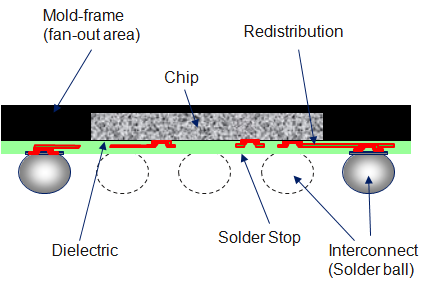
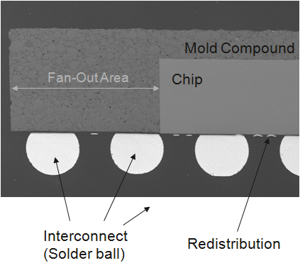
303:(eWLB) is a packaging technology for integrated circuits. The package interconnects are applied on an artificial wafer made of silicon chips and a casting compound.
499:
https://web.archive.org/web/20080517033548/http://www.ciol.com/Semicon/Tech-Watch/News-Reports/Infineon,-ASE-intro-eWLB-package-technology/131107101404/0/
972:
503:
541:
350:) the electrical connections from the chip pads to the interconnects are made in thin-film technology, as for any other classical wafer level package.
321:
All process steps for the generation of the package are performed on the wafer. This allows, in comparison to classical packaging technologies (e. g.
44:
130:
536:
102:
375:
522:
109:
884:
570:
333:
178:
484:
https://web.archive.org/web/20120305094749/http://www.infineonventures.com/cms/en/corporate/press/news/releases/2007/INFCOM200711-013.html
247:
189:
307:
116:
941:
821:
287:
269:
207:
149:
52:
811:
806:
98:
563:
329:) fit on the chip (so called fan-in design). Therefore only chips with a restricted number of interconnects can be packaged.
87:
615:
967:
850:
504:
http://www.statschippac.com/services/packagingservices/waferlevelproducts/~/media/Files/Package%20Datasheets/eWLB.ashx
346:
dies for carrying additional interconnect elements is created. After the build of the artificial wafer (the so-called
998:
It is relatively common to find packages that contain other components than their designated ones, such as diodes or
240:
234:
542:
https://web.archive.org/web/20090728202431/http://annualreport2008.infineon.com/de/template.asp?content=innovationen
855:
816:
801:
786:
318:). The main driving force behind the eWLB technology was to allow fanout and more space for interconnect routing.
123:
76:
251:
982:
646:
537:
https://web.archive.org/web/20110703111509/http://141.30.122.65/Keynotes/6-Plieninger-ESTC_Keynote_20060907.pdf
488:
987:
826:
1019:
796:
770:
977:
946:
586:
466:
355:
182:
that states a
Knowledge (XXG) editor's personal feelings or presents an original argument about a topic.
431:
Mechanical stress between package and board is transmitted stronger than for other package technologies
962:
845:
791:
638:
493:
904:
627:
315:
314:
eWLB is a further development of the classical wafer level ball grid array technology (WLB or WLP:
518:
931:
921:
441:
359:
999:
860:
381:
362:
and STATS ChipPAC Ltd. First components were brought into market mid of 2009 (mobile phone).
753:
747:
741:
729:
717:
711:
699:
603:
513:
936:
889:
879:
526:
446:
322:
508:
894:
1013:
354:
number of interconnects at a suitable distance. The eWLB technology was developed by
332:
326:
65:
531:
342:
926:
549:
Thermal and
Electrical Characterization of eWLB (embedded Wafer Level BGA),
489:
http://content.yudu.com/Library/A1mxrk/3DPackagingFebruaryi/resources/4.htm
306:
555:
735:
723:
705:
693:
621:
609:
428:
Inspection and repair difficult since visual inspection is restricted
412:
Number of realizable interconnects on the package is not restricted
687:
681:
675:
669:
595:
494:
https://safe.nrao.edu/pub/Main/EuropeanMicrowaveWeek08/WFR14-1.pdf
663:
657:
651:
559:
415:
High integration potential for multi-die- and stacked packages
219:
161:
59:
18:
552:
Electronic
Components and Technology Conference (ECTC), 2010
179:
personal reflection, personal essay, or argumentative essay
514:
http://www.wsdmag.com/Articles/ArticleID/19576/19576.html
185:
509:
http://www.amkor.com/go/packaging/all-packages/cspnl/
467:"Infineon, ST and STATS Develops eWLB | TopNews"
955:
903:
872:
835:
779:
763:
637:
593:
90:. Unsourced material may be challenged and removed.
371:Lamination of foil onto carrier (lamination tool)
571:
8:
532:https://ieeexplore.ieee.org/document/4147210
16:Packaging technology for integrated circuits
409:Excellent electrical and thermal properties
53:Learn how and when to remove these messages
973:List of integrated circuit packaging types
578:
564:
556:
288:Learn how and when to remove this message
270:Learn how and when to remove this message
208:Learn how and when to remove this message
150:Learn how and when to remove this message
331:
305:
233:This article includes a list of general
630:(SOD-123 / SOD-323 / SOD-523 / SOD-923)
458:
406:Minimal lateral package size and height
387:De-bonding of carrier (de-bonding tool)
99:"Embedded wafer level ball grid array"
7:
301:Embedded wafer level ball grid array
88:adding citations to reliable sources
521:Francoise von Trapp, Nov. 30, 2009
239:it lacks sufficient corresponding
14:
34:This article has multiple issues.
224:
166:
64:
23:
393:Ball drop reflow and wafer test
75:needs additional citations for
42:or discuss these issues on the
612:(DO-7 / DO-26 / DO-35 / DO-41)
1:
1002:in transistor packages, etc.
968:Integrated circuit packaging
403:Low cost (package and test)
374:Chip placement onto wafer (
1036:
996:
418:Upcoming package standard
983:Surface-mount technology
390:Flip reconstructed wafer
988:Through-hole technology
546:Seung Wook Yoon et al.
254:more precise citations.
618:(MELF / SOD-80 / LL34)
587:Semiconductor packages
519:eWLB hits the big time
337:
311:
188:by rewriting it in an
978:Printed circuit board
335:
309:
963:Electronic packaging
84:improve this article
316:wafer level package
1000:voltage regulators
525:2012-03-04 at the
442:Chip-scale package
360:STMicroelectronics
338:
336:Cross-section eWLB
312:
190:encyclopedic style
177:is written like a
1007:
1006:
756:(Super-247) (SMT)
750:(Super-220) (SMT)
624:(SMA / SMB / SMC)
298:
297:
290:
280:
279:
272:
218:
217:
210:
160:
159:
152:
134:
57:
1027:
580:
573:
566:
557:
471:
470:
463:
293:
286:
275:
268:
264:
261:
255:
250:this article by
241:inline citations
228:
227:
220:
213:
206:
202:
199:
193:
170:
169:
162:
155:
148:
144:
141:
135:
133:
92:
68:
60:
49:
27:
26:
19:
1035:
1034:
1030:
1029:
1028:
1026:
1025:
1024:
1010:
1009:
1008:
1003:
992:
951:
899:
868:
831:
775:
759:
633:
589:
584:
527:Wayback Machine
480:
475:
474:
465:
464:
460:
455:
447:Ball grid array
438:
425:
400:
368:
323:ball grid array
294:
283:
282:
281:
276:
265:
259:
256:
246:Please help to
245:
229:
225:
214:
203:
197:
194:
186:help improve it
183:
171:
167:
156:
145:
139:
136:
93:
91:
81:
69:
28:
24:
17:
12:
11:
5:
1033:
1031:
1023:
1022:
1012:
1011:
1005:
1004:
997:
994:
993:
991:
990:
985:
980:
975:
970:
965:
959:
957:
956:Related topics
953:
952:
950:
949:
944:
939:
934:
929:
924:
919:
916:
913:
909:
907:
901:
900:
898:
897:
892:
887:
882:
876:
874:
870:
869:
867:
866:
863:
858:
853:
848:
843:
839:
837:
833:
832:
830:
829:
824:
822:TSSOP / HTSSOP
819:
814:
809:
804:
799:
794:
789:
783:
781:
777:
776:
774:
773:
767:
765:
761:
760:
758:
757:
751:
745:
739:
733:
727:
721:
715:
709:
703:
697:
691:
685:
679:
673:
667:
661:
655:
649:
643:
641:
635:
634:
632:
631:
625:
619:
613:
607:
600:
598:
591:
590:
585:
583:
582:
575:
568:
560:
554:
553:
544:
539:
534:
529:
516:
511:
506:
501:
496:
491:
486:
479:
478:External links
476:
473:
472:
457:
456:
454:
451:
450:
449:
444:
437:
434:
433:
432:
429:
424:
421:
420:
419:
416:
413:
410:
407:
404:
399:
396:
395:
394:
391:
388:
385:
379:
376:pick and place
372:
367:
364:
348:reconstitution
310:Principle eWLB
296:
295:
278:
277:
232:
230:
223:
216:
215:
174:
172:
165:
158:
157:
72:
70:
63:
58:
32:
31:
29:
22:
15:
13:
10:
9:
6:
4:
3:
2:
1032:
1021:
1020:Chip carriers
1018:
1017:
1015:
1001:
995:
989:
986:
984:
981:
979:
976:
974:
971:
969:
966:
964:
961:
960:
958:
954:
948:
945:
943:
940:
938:
935:
933:
930:
928:
925:
923:
920:
917:
914:
911:
910:
908:
906:
902:
896:
893:
891:
888:
886:
883:
881:
878:
877:
875:
871:
864:
862:
859:
857:
854:
852:
849:
847:
844:
841:
840:
838:
834:
828:
825:
823:
820:
818:
815:
813:
810:
808:
805:
803:
800:
798:
795:
793:
790:
788:
785:
784:
782:
778:
772:
769:
768:
766:
762:
755:
752:
749:
746:
744:(D3PAK) (SMT)
743:
740:
738:(D2PAK) (SMT)
737:
734:
732:(I2PAK) (SMT)
731:
728:
725:
722:
719:
716:
713:
710:
707:
704:
701:
698:
695:
692:
689:
686:
683:
680:
677:
674:
671:
668:
665:
662:
659:
656:
653:
650:
648:
645:
644:
642:
640:
636:
629:
626:
623:
620:
617:
614:
611:
608:
605:
602:
601:
599:
597:
592:
588:
581:
576:
574:
569:
567:
562:
561:
558:
551:
550:
545:
543:
540:
538:
535:
533:
530:
528:
524:
520:
517:
515:
512:
510:
507:
505:
502:
500:
497:
495:
492:
490:
487:
485:
482:
481:
477:
468:
462:
459:
452:
448:
445:
443:
440:
439:
435:
430:
427:
426:
423:Disadvantages
422:
417:
414:
411:
408:
405:
402:
401:
397:
392:
389:
386:
383:
380:
377:
373:
370:
369:
366:Process Steps
365:
363:
361:
357:
351:
349:
344:
334:
330:
328:
324:
319:
317:
308:
304:
302:
292:
289:
274:
271:
263:
253:
249:
243:
242:
236:
231:
222:
221:
212:
209:
201:
191:
187:
181:
180:
175:This article
173:
164:
163:
154:
151:
143:
132:
129:
125:
122:
118:
115:
111:
108:
104:
101: –
100:
96:
95:Find sources:
89:
85:
79:
78:
73:This article
71:
67:
62:
61:
56:
54:
47:
46:
41:
40:
35:
30:
21:
20:
947:WL-CSP / WLP
817:TSOP / HTSOP
726:(DPAK) (SMT)
720:(IPAK) (SMT)
714:(TH / Panel)
708:(TH / Panel)
702:(TH / Panel)
696:(TH / Panel)
684:(TH / Panel)
654:(TH / Panel)
548:
461:
384:(mold press)
352:
347:
339:
327:solder balls
320:
313:
300:
299:
284:
266:
257:
238:
204:
195:
176:
146:
137:
127:
120:
113:
106:
94:
82:Please help
77:verification
74:
50:
43:
37:
36:Please help
33:
865:QUIP / QUIL
252:introducing
873:Grid array
812:SOP / SSOP
764:Single row
647:SOT / TSOT
453:References
398:Advantages
343:singulated
260:March 2010
235:references
198:March 2010
140:March 2010
110:newspapers
39:improve it
927:Flip Chip
846:QIP / QIL
807:SO / SOIC
797:Flat Pack
792:DIP / DIL
771:SIP / SIL
639:3...5-pin
45:talk page
1014:Category
836:Quad row
780:Dual row
523:Archived
436:See also
356:Infineon
606:(DO-27)
594:Single
382:Molding
248:improve
184:Please
124:scholar
754:TO-274
748:TO-273
742:TO-268
736:TO-263
730:TO-262
724:TO-252
718:TO-251
712:TO-247
706:TO-220
700:TO-202
694:TO-126
622:DO-214
616:DO-213
610:DO-204
604:DO-201
237:, but
126:
119:
112:
105:
97:
905:Wafer
688:TO-92
682:TO-66
676:TO-39
670:TO-18
596:diode
378:tool)
131:JSTOR
117:books
942:UICC
885:eWLB
851:PLCC
802:MSOP
690:(TH)
678:(TH)
672:(TH)
666:(TH)
664:TO-8
660:(TH)
658:TO-5
652:TO-3
103:news
932:PoP
922:CSP
918:COG
915:COF
912:COB
895:PGA
890:LGA
880:BGA
861:QFP
856:QFN
842:LCC
827:ZIP
787:DFN
628:SOD
86:by
1016::
937:QP
358:,
48:.
579:e
572:t
565:v
469:.
291:)
285:(
273:)
267:(
262:)
258:(
244:.
211:)
205:(
200:)
196:(
192:.
153:)
147:(
142:)
138:(
128:·
121:·
114:·
107:·
80:.
55:)
51:(
Text is available under the Creative Commons Attribution-ShareAlike License. Additional terms may apply.