24:
227:
voltage, and once the applied voltage exceeds this value charge neutrality is achieved almost entirely by addition of electrons to the inversion layer rather than by an increase in acceptor ion charge by expansion of the depletion layer. Further field penetration into the semiconductor is arrested at
187:
in the valence band. Charge neutrality prevails in the field-free region because a negative acceptor ion creates a positive deficiency in the host material: a hole is the absence of an electron, it behaves like a positive charge. Where no field is present, neutrality is achieved because the negative
218:
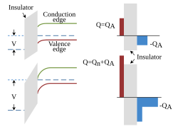
The conduction band edge also is lowered, increasing electron occupancy of these states, but at low voltages this increase is not significant. At larger applied voltages, however, as in the bottom panel, the conduction band edge is lowered sufficiently to cause significant population of these levels
196:
Next the band bending is described. A positive charge is placed on the left face of the insulator (for example using a metal "gate" electrode). In the insulator there are no charges so the electric field is constant, leading to a linear change of voltage in this material. As a result, the insulator
101:
The change in surface conductance occurs because the applied field alters the energy levels available to electrons to considerable depths from the surface, and that in turn changes the occupancy of the energy levels in the surface region. A typical treatment of such effects is based upon a
205:
where the bulk occupancy reestablishes itself because the field cannot penetrate further. Because the valence band levels near the surface are fully occupied due to the lowering of these levels, only the immobile negative acceptor-ion charges are present near the surface, which becomes an
177:
The example in the figure shows the Fermi level in the bulk material beyond the range of the applied field as lying close to the valence band edge. This position for the occupancy level is arranged by introducing impurities into the semiconductor. In this case the impurities are so-called
210:). Thus, field penetration is arrested when the exposed negative acceptor ion charge balances the positive charge placed on the insulator surface: the depletion layer adjusts its depth enough to make the net negative acceptor ion charge balance the positive charge on the gate.
348:
34:, left). The charge inducing the bending is balanced by a layer of negative acceptor-ion charge (right). Bottom panel: A larger applied voltage further depletes holes but conduction band lowers enough in energy to populate an inversion layer.
200:
In the semiconductor at the smaller voltage shown in the top panel, the positive charge placed on the left face of the insulator lowers the energy of the valence band edge. Consequently, these states are fully occupied out to a so-called
69:) that can respond to an applied field is sufficiently small that the field can penetrate quite far into the material. This field penetration alters the conductivity of the semiconductor near its surface, and is called the
182:
which soak up electrons from the valence band becoming negatively charged, immobile ions embedded in the semiconductor material. The removed electrons are drawn from the valence band levels, leaving vacancies or
223:
layer because the electrons are opposite in polarity to the holes originally populating the semiconductor. This onset of electron charge in the inversion layer becomes very significant at an applied
352:
57:, the electron density that responds to applied fields is so large that an external electric field can penetrate only a very short distance into the material. However, in a
169:
the states are more likely to be occupied, the conduction band moves closer to the Fermi level, indicating more electrons are in the conducting band near the insulator.
383:
326:
378:
373:
17:
228:
this point, as the electron density increases exponentially with band-bending beyond the threshold voltage, effectively
154:
197:
conduction and valence bands are therefore straight lines in the figure, separated by the large insulator energy gap.
388:
368:
128:
78:
43:
153:). The left panels show the lowest energy level of the conduction band and the highest energy level of the
344:
311:"Chapter 10: Metal semiconductor contacts: Metal semiconductor and junction field effect transistors"
131:
as left-hand layer and a semiconductor as right-hand layer. An example of such a structure is the
161:. By convention, the energy of electrons is shown, so a positive voltage penetrating the surface
115:
An example band-bending diagram is shown in the figure. For convenience, energy is expressed in
23:
322:
310:
124:
393:
146:
74:
47:
362:
133:
66:
58:
145:(such as silicon) with a body contact, and an intervening insulating layer (such as
116:
103:
31:
340:
166:
165:
the conduction edge. A dashed line depicts the occupancy situation: below this
30:: Top panels: An applied voltage bends bands, depleting holes from surface (
62:
90:
82:
157:. These levels are "bent" by the application of a positive voltage
127:. In the figure, a two-layer structure is shown, consisting of an
119:
and voltage is expressed in volts, avoiding the need for a factor
54:
86:
232:
the depletion layer depth at its value at threshold voltages.
349:
Creative
Commons Attribution-ShareAlike 3.0 Unported License
206:electrically insulating region without holes (the
188:acceptor ions exactly balance the positive holes.
73:. The field effect underlies the operation of the
46:of a material by the application of an external
307:ransistor. For a discussion see, for example,
137:, a two-terminal structure made up of a metal
8:
339:This article incorporates material from the
112:as a function of depth into the material.
22:
240:
108:showing the positions in energy of the
315:Fundamentals of semiconductor devices
219:in a narrow surface layer, called an
7:
97:Surface conductance and band bending
14:
317:. Tata McGraw-Hill. pp. 475
42:refers to the modulation of the
347:", which is licensed under the
309:M K Achuthan K N Bhat (2007).
1:
410:
384:Electronic band structures
15:
345:Field effect#Field effect
141:contact, a semiconductor
379:Semiconductor structures
374:Semiconductor technology
149:, hence the designation
79:field-effect transistors
247:The acronyms stand for
44:electrical conductivity
35:
61:the lower density of
26:
105:band-bending diagram
16:For other uses, see
389:Physical phenomena
351:but not under the
36:
125:elementary charge
401:
333:
332:
245:
38:In physics, the
409:
408:
404:
403:
402:
400:
399:
398:
359:
358:
336:
329:
308:
287:ransistor, and
246:
242:
238:
216:
208:depletion layer
203:depletion depth
194:
175:
147:silicon dioxide
99:
21:
12:
11:
5:
407:
405:
397:
396:
391:
386:
381:
376:
371:
369:Semiconductors
361:
360:
335:
334:
328:978-0070612204
327:
239:
237:
234:
215:
212:
193:
192:Surface region
190:
174:
171:
98:
95:
81:, notably the
75:Schottky diode
65:(and possibly
48:electric field
13:
10:
9:
6:
4:
3:
2:
406:
395:
392:
390:
387:
385:
382:
380:
377:
375:
372:
370:
367:
366:
364:
357:
356:
354:
350:
346:
342:
330:
324:
320:
316:
312:
306:
302:
298:
295:emiconductor
294:
290:
286:
282:
278:
274:
270:
266:
262:
259:emiconductor
258:
254:
250:
244:
241:
235:
233:
231:
226:
222:
213:
211:
209:
204:
198:
191:
189:
186:
181:
172:
170:
168:
164:
160:
156:
152:
148:
144:
140:
136:
135:
134:MOS capacitor
130:
126:
122:
118:
113:
111:
107:
106:
96:
94:
92:
88:
84:
80:
76:
72:
68:
64:
60:
59:semiconductor
56:
51:
49:
45:
41:
33:
29:
25:
19:
338:
337:
318:
314:
304:
300:
296:
292:
288:
284:
280:
276:
272:
268:
264:
260:
256:
252:
248:
243:
229:
224:
220:
217:
207:
202:
199:
195:
184:
179:
176:
162:
158:
155:valence band
150:
142:
138:
132:
120:
114:
109:
104:
100:
71:field effect
70:
52:
40:field effect
39:
37:
32:band diagram
28:Field effect
27:
18:Field effect
341:Citizendium
271:ransistor,
173:Bulk region
167:Fermi level
363:Categories
236:References
110:band edges
343:article "
225:threshold
221:inversion
214:Inversion
180:acceptors
129:insulator
63:electrons
275:unction
123:for the
89:and the
394:MOSFETs
230:pinning
77:and of
325:
303:ffect
283:ffect
267:ffect
163:lowers
91:MESFET
85:, the
83:MOSFET
299:ield
279:ield
263:ield
255:xide
251:etal
185:holes
67:holes
55:metal
53:In a
353:GFDL
323:ISBN
291:tal
143:body
139:gate
87:JFET
93:.
365::
321:.
319:ff
313:.
289:ME
117:eV
50:.
355:.
331:.
305:T
301:E
297:F
293:S
285:T
281:E
277:F
273:J
269:T
265:E
261:F
257:S
253:O
249:M
159:V
151:O
121:q
20:.
Text is available under the Creative Commons Attribution-ShareAlike License. Additional terms may apply.