167:
an electrostatically actuated device, similar to
Espinosa’s original design, was developed in Silicon-On-Insulator technology by the Michler’s group. These devices have the advantage of a higher aspect ratio and therefore a higher sensitivity in the sensing structures. Some other researchers have developed other devices following the models outlines by Espinosa, Saif and Haque; for example Victor Bright at University of Colorado – Boulder. The technology has reached a level of maturity such that standard devices are now offered by the Center for Integrated Nanotechnologies (CINT) at Sandia National Labs to researchers interested in mechanical testing of nanoscale samples.
151:
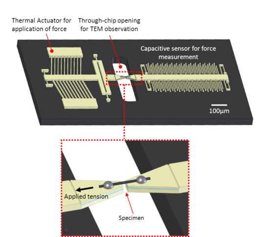
University. They designed and developed a true MEM system that incorporated capacitive sensing for electronic measurement of load and thermal actuation for specimen straining in one single chip. The system could be operated inside a transmission electron microscope. The MEMS based platform was applied to the study of poly-Silicon samples, multi-walled CNTs and more recently metallic and semiconducting nanowires. In particular, the theoretical strength of carbon nanotubes was experimentally measured for the first time using this device.
114:(AFM) to perform a three-point bending test, SEM and TEM to perform bending resonance tests and nanoindenters to perform compression tests. In recent years, it has been found that results are not completely unambiguous. This was exemplified by the fact that different researchers obtained different values of the same property for the same material. This spurred the development of MEMS with the capability of carrying out tensile tests on individual nanoscale elements.
188:
biological systems finds application in disease diagnosis and treatment, and in the engineering of new materials. The size scales in biological testing are in the micron range, with structures that are typically very compliant. This requires the development of devices with high displacement capabilities and very high force resolution. Recent examples are the tensile characterization of collagen fibrils and DNA bundles.
155:
175:
Several nanomechanical characterization methods have yielded many results for properties of matter at the nanoscale. What has been found consistently is that mechanical properties of materials change as a function of size. In metals, elastic modulus, yield strength and fracture strength all increase,
166:
Following these pioneering works, other research groups have followed on developing their own MEMS for mechanical testing. Important examples include the deBoer group at Sandia
National Labs who specializes in the testing of polysilicon samples. At the Ecole Polythecnique Federale de Lausanne (EPFL),
105:
Typical macroscale mechanical characterization is mostly performed under uniaxial tensile conditions. Despite the existence of other methods of mechanical characterization such as three-point bending, hardness testing, etc., uniaxial tensile testing allows for the measurement of the most fundamental
150:
SEM and TEM were demonstrated for thin films by his group including a stage for simultaneous electrical and mechanical testing, although this set-up used external actuation and sensing. A major breakthrough in MEMS-electronic integration was made by
Horacio D. Espinosa and his group at Northwestern
187:
On the other hand, given that MEMS has demonstrated to be a feasible technology for characterizing mechanical properties at the nanoscale, application of the technology to other types of problems has been sought. In particular, biological systems spur an interest because understanding mechanics in
179:
The discovery that mechanical properties are intrinsically size-dependent has spurred theoretical and experimental interest in the size-dependence of other material properties, such as thermal and electrical; and also coupled effects like electromechanical or thermomechanical behavior. Particular
109:
At the nanoscale, owing to the reduced size of the specimen and the forces and displacements to be measured, uniaxial testing or any mechanical testing for that matter, are challenging. As a result, most tests are carried in configurations other than uniaxial-tensile, using available nanoscale
106:
mechanical measurement of the specimen, namely its stress-strain curve. From this curve, important properties like the Young’s modulus, Yield strength, Fracture
Strength can be computed. Other properties such as toughness and ductility can be computed as well.
766:
Bernal, R.A., R. Agrawal, B. Peng, K.A. Bertness, N.A. Sanford, A.V. Davydov, and H.D. Espinosa (2010). "Effect of Growth
Orientation and Diameter on the Elasticity of GaN Nanowires. A Combined in Situ TEM and Atomistic Modeling Investigation".
134:, which were fabricated by standard machining techniques. However, important contributions and insights were provided into specimen gripping mechanisms and the mechanics of materials at the micron scale. Likewise, Horacio D. Espinosa at
659:
Peng, B., M. Locascio, P. Zapol, S. Li, S.L. Mielke, G.C. Schatz, and H.D. Espinosa (2008). "Measurements of near-ultimate strength for multiwalled carbon nanotubes and irradiation-induced crosslinking improvements".
96:
mechanical testing coupled with other type of measurements, such as electrical or thermal, and to extend the range of samples tested to the biological domain, testing specimens such as cells and collagen fibrils.
138:
developed a membrane deflection experiment, which was employed at the MEMS level as well as in thin film specimens. The latest revealed the first experimental evidence of size scale plasticity in thin metallic
863:
Zhang, Dongfeng; Breguet, Jean-Marc; Clavel, Reymond; Philippe, Laetitia; Utke, Ivo; Michler, Johann (2009). "In situ tensile testing of individual Co nanowires inside a scanning electron microscope".
1150:
Yamahata, C., D. Collard, B. Legrand, T. Takekawa, M. Kumemura, G. Hashiguchi, and H. Fujita (2008). "Silicon
Nanotweezers With Subnanometer Resolution for the Micromanipulation of Biomolecules".
85:
can be used to further characterize the sample, providing a complete picture of the evolution of the specimen as it is loaded and fails. Owing to the development of mature MEMS
180:
interest has been focused on characterizing electromechanical properties such as piezoresistivity and piezoelectricity. Most of the current focus in the developing of MEMS for
914:
Brown, J.J., A.I. Baca, K.A. Bertness, D.A. Dikin, R.S. Ruoff, and V.M. Bright (2011). "Tensile measurement of single crystal gallium nitride nanowires on MEMS test stages".
130:
conducted pioneering work in the testing of microscale specimen of polycrystalline silicon. Some of the initial developments consisted mostly of miniaturized versions of
1185:
1136:
1065:
1002:
941:
810:
752:
695:
642:
423:
374:
318:
54:. They distinguish themselves from other methods of nanomechanical testing because the sensing and actuation mechanisms are embedded and/or co-fabricated in the
709:
Agrawal, R., B. Peng, E.E. Gdoutos, and H.D. Espinosa (2008). "Elasticity size effects in ZnO nanowires – A combined
Experimental-Computational approach".
388:
Espinosa, H.D., B.C. Prorok, and B. Peng (2004). "Plasticity size effects in free-standing submicron polycrystalline FCC films subjected to pure tension".
143:
films. Later, size effect studies were performed on single crystal pillars using nanoindentation of microfabricated samples by means of focused ion beam.
283:
Espinosa, H.D., B.C. Prorok, and M. Fischer (2003). "A methodology for determining mechanical properties of freestanding thin films and MEMS materials".
605:
Peng, B., Y.G. Sun, Y. Zhu, H.-H. Wang, and H.D. Espinosa (2008). "Nanoscale testing of One-dimensional nanostructures". In F. Yang; C.J.M. Li (eds.).
122:
The interest in nanomechanical testing was initially spurred by a need to characterize the materials that were used in the fabrication of MEMS.
505:
Han, J.H. & M.T.A. Saif (2006). "In situ microtensile stage for electromechanical characterization of nanoscale freestanding films".
146:
Later on, Taher Saif at
University of Illinois- Urbana Champaign can be credited on developing microfabricated stages. Several results
967:
Haque, M.A., H.D. Espinosa, and H.J. Lee (2010). "MEMS for In Situ
Testing – Handling, Actuation, Loading, Displacement Measurement".
626:
74:
27:
70:
176:
while in semiconducting brittle materials, either increments or reductions are observed depending on the material.
333:
131:
334:"An Experimental/Computational approach to identify Moduli and Residual Stress in MEMS Radio-Frequency Switches"
127:
221:
Agrawal, R. & Espinosa, H.D. (2009). "Multiscale
Experiments: State of the Art and Remaining Challenges".
65:, i.e., testing while observing the evolution of the sample in high magnification instruments such as optical
1204:
135:
111:
1179:
1130:
1059:
996:
935:
804:
746:
689:
470:
Haque, M.A. & M.T.A. Saif (2002). "In-situ tensile testing of nano-scale specimens in SEM and TEM".
417:
368:
312:
89:
technologies, the use of these microsystems for research purposes has been increasing in recent years.
1092:
872:
776:
718:
556:
514:
397:
292:
31:
61:
This level of integration and miniaturization allows carrying out the mechanical characterization
1167:
984:
896:
845:
636:
487:
356:
238:
545:"An electromechanical material testing system for in situ electron microscopy and applications"
1118:
1047:
888:
792:
734:
677:
622:
584:
123:
35:
1159:
1108:
1100:
1037:
1029:
976:
923:
880:
837:
784:
726:
669:
614:
606:
574:
564:
522:
479:
450:
405:
348:
300:
265:
230:
86:
39:
77:(TEM) and X-ray setups. Furthermore, analytical capabilities of these instruments such as
1018:"Nano measurements with micro-devices: mechanical properties of hydrated collagen fibrils"
884:
1096:
876:
841:
780:
722:
560:
518:
401:
296:
154:
1113:
1080:
1042:
1017:
579:
544:
304:
1198:
849:
607:
491:
455:
438:
197:
1171:
988:
900:
360:
242:
1079:
Shen, Z.L., Kahn, H., Ballarini, R., Eppell, S.J.; Kahn; Ballarini; Eppell (2011).
78:
618:
954:
82:
55:
549:
Proceedings of the National Academy of Sciences of the United States of America
409:
1163:
1104:
927:
269:
66:
569:
51:
43:
1122:
1051:
1033:
892:
796:
738:
681:
673:
588:
47:
980:
256:
Sharpe, W.N. (2008). "A review of tension test methods for thin films".
184:
testing lies in this area with examples from Haque, Espinosa and Zhang.
58:, providing—in the majority of cases—greater sensitivity and precision.
483:
352:
788:
730:
526:
234:
153:
332:
Espinosa, H.D., Y. Zhu, M. Fischer, and J. Hutchinson (2003).
30:(MEMS) used to measure the mechanical properties (such as the
16:
MEMS that measure mechanical properties of nanoscale objects
1016:
Eppell, S.J., Smith, B.N., Kahn, H., Ballarini, R. (2006).
609:
Micro and Nano Mechanical Testing of Materials and Devices
1081:"Viscoelastic Properties of Isolated Collagen Fibrils"
92:Most of the current developments aim to implement
223:Journal of Engineering Materials and Technology
830:Journal of Micromechanics and Microengineering
390:Journal of the Mechanics and Physics of Solids
285:Journal of the Mechanics and Physics of Solids
824:Siddharth, S.H. (2009). "Demonstration of an
8:
1184:: CS1 maint: multiple names: authors list (
1135:: CS1 maint: multiple names: authors list (
1064:: CS1 maint: multiple names: authors list (
1001:: CS1 maint: multiple names: authors list (
940:: CS1 maint: multiple names: authors list (
809:: CS1 maint: multiple names: authors list (
751:: CS1 maint: multiple names: authors list (
694:: CS1 maint: multiple names: authors list (
641:: CS1 maint: multiple names: authors list (
422:: CS1 maint: multiple names: authors list (
373:: CS1 maint: multiple names: authors list (
317:: CS1 maint: multiple names: authors list (
101:Mechanical characterization at the nanoscale
437:Saif, M.T.A. & MacDonald, N.C. (1996).
1152:Journal of Microelectromechanical Systems
1112:
1041:
578:
568:
454:
208:
118:Historical context and state of the art
1177:
1128:
1057:
1022:Journal of the Royal Society Interface
994:
933:
802:
744:
687:
634:
415:
366:
310:
654:
652:
600:
598:
543:Zhu, Y. & Espinosa, H.D. (2005).
7:
538:
536:
216:
214:
212:
439:"A millinewton microloading device"
14:
162:tensile testing of nanostructures
75:transmission electron microscopes
507:Review of Scientific Instruments
885:10.1088/0957-4484/20/36/365706
613:. Springer. pp. 280–304.
28:microelectromechanical systems
1:
842:10.1088/0960-1317/19/8/082001
305:10.1016/S0022-5096(02)00062-5
71:scanning electron microscopes
619:10.1007/978-0-387-78701-5_11
456:10.1016/0924-4247(96)80127-0
24:mechanical characterization
1221:
410:10.1016/j.jmps.2003.07.001
158:Schematic of the MEMS for
132:universal testing machines
50:, whiskers, nanotubes and
1164:10.1109/JMEMS.2008.922080
1105:10.1016/j.bpj.2011.04.052
928:10.1016/j.sna.2010.04.002
828:on-chip tensile tester".
270:10.1557/PROC-1052-DD01-01
128:Johns Hopkins University
916:Sensors and Actuators A
570:10.1073/pnas.0506544102
443:Sensors and Actuators A
229:(4): 0412081–04120815.
136:Northwestern University
112:atomic force microscope
110:science tools like the
1034:10.1098/rsif.2005.0100
957:. cint.lanl.gov (2009)
674:10.1038/nnano.2008.211
472:Experimental Mechanics
341:Experimental Mechanics
163:
662:Nature Nanotechnology
157:
1097:2011BpJ...100.3008S
1085:Biophysical Journal
981:10.1557/mrs2010.570
955:Discovery Platforms
877:2009Nanot..20J5706Z
781:2011NanoL..11..548B
723:2008NanoL...8.3668A
561:2005PNAS..10214503Z
555:(41): 14503–14508.
519:2006RScI...77d5102H
402:2004JMPSo..52..667E
297:2003JMPSo..51...47E
484:10.1007/BF02411059
353:10.1007/BF02410529
164:
42:specimens such as
1091:(12): 3008–3015.
789:10.1021/nl103450e
731:10.1021/nl801724b
717:(11): 3668–3674.
527:10.1063/1.2188368
235:10.1115/1.3183782
171:Future directions
124:William N. Sharpe
36:fracture strength
1212:
1190:
1189:
1183:
1175:
1147:
1141:
1140:
1134:
1126:
1116:
1076:
1070:
1069:
1063:
1055:
1045:
1013:
1007:
1006:
1000:
992:
964:
958:
952:
946:
945:
939:
931:
911:
905:
904:
860:
854:
853:
821:
815:
814:
808:
800:
763:
757:
756:
750:
742:
706:
700:
699:
693:
685:
656:
647:
646:
640:
632:
612:
602:
593:
592:
582:
572:
540:
531:
530:
502:
496:
495:
467:
461:
460:
458:
434:
428:
427:
421:
413:
385:
379:
378:
372:
364:
338:
329:
323:
322:
316:
308:
280:
274:
273:
253:
247:
246:
218:
87:microfabrication
1220:
1219:
1215:
1214:
1213:
1211:
1210:
1209:
1195:
1194:
1193:
1176:
1149:
1148:
1144:
1127:
1078:
1077:
1073:
1056:
1015:
1014:
1010:
993:
966:
965:
961:
953:
949:
932:
913:
912:
908:
862:
861:
857:
823:
822:
818:
801:
765:
764:
760:
743:
708:
707:
703:
686:
668:(10): 626–631.
658:
657:
650:
633:
629:
604:
603:
596:
542:
541:
534:
513:(4): 045102–8.
504:
503:
499:
469:
468:
464:
436:
435:
431:
414:
387:
386:
382:
365:
336:
331:
330:
326:
309:
282:
281:
277:
258:MRS Proceedings
255:
254:
250:
220:
219:
210:
206:
194:
173:
120:
103:
32:Young’s modulus
17:
12:
11:
5:
1218:
1216:
1208:
1207:
1205:Nanotechnology
1197:
1196:
1192:
1191:
1158:(3): 623–631.
1142:
1071:
1028:(6): 117–121.
1008:
959:
947:
922:(2): 177–186.
906:
871:(36): 365706.
865:Nanotechnology
855:
816:
758:
701:
648:
628:978-0387787008
627:
594:
532:
497:
478:(1): 123–128.
462:
449:(1–3): 65–75.
429:
396:(3): 667–689.
380:
347:(3): 309–316.
324:
275:
248:
207:
205:
202:
201:
200:
193:
190:
172:
169:
119:
116:
102:
99:
15:
13:
10:
9:
6:
4:
3:
2:
1217:
1206:
1203:
1202:
1200:
1187:
1181:
1173:
1169:
1165:
1161:
1157:
1153:
1146:
1143:
1138:
1132:
1124:
1120:
1115:
1110:
1106:
1102:
1098:
1094:
1090:
1086:
1082:
1075:
1072:
1067:
1061:
1053:
1049:
1044:
1039:
1035:
1031:
1027:
1023:
1019:
1012:
1009:
1004:
998:
990:
986:
982:
978:
974:
970:
963:
960:
956:
951:
948:
943:
937:
929:
925:
921:
917:
910:
907:
902:
898:
894:
890:
886:
882:
878:
874:
870:
866:
859:
856:
851:
847:
843:
839:
836:(8): 082001.
835:
831:
827:
820:
817:
812:
806:
798:
794:
790:
786:
782:
778:
775:(2): 548–55.
774:
770:
762:
759:
754:
748:
740:
736:
732:
728:
724:
720:
716:
712:
705:
702:
697:
691:
683:
679:
675:
671:
667:
663:
655:
653:
649:
644:
638:
630:
624:
620:
616:
611:
610:
601:
599:
595:
590:
586:
581:
576:
571:
566:
562:
558:
554:
550:
546:
539:
537:
533:
528:
524:
520:
516:
512:
508:
501:
498:
493:
489:
485:
481:
477:
473:
466:
463:
457:
452:
448:
444:
440:
433:
430:
425:
419:
411:
407:
403:
399:
395:
391:
384:
381:
376:
370:
362:
358:
354:
350:
346:
342:
335:
328:
325:
320:
314:
306:
302:
298:
294:
290:
286:
279:
276:
271:
267:
263:
259:
252:
249:
244:
240:
236:
232:
228:
224:
217:
215:
213:
209:
203:
199:
198:Lab-on-a-chip
196:
195:
191:
189:
185:
183:
177:
170:
168:
161:
156:
152:
149:
144:
142:
137:
133:
129:
125:
117:
115:
113:
107:
100:
98:
95:
90:
88:
84:
80:
76:
72:
68:
64:
59:
57:
53:
49:
45:
41:
37:
33:
29:
25:
23:
1180:cite journal
1155:
1151:
1145:
1131:cite journal
1088:
1084:
1074:
1060:cite journal
1025:
1021:
1011:
997:cite journal
972:
969:MRS Bulletin
968:
962:
950:
936:cite journal
919:
915:
909:
868:
864:
858:
833:
829:
825:
819:
805:cite journal
772:
769:Nano Letters
768:
761:
747:cite journal
714:
711:Nano Letters
710:
704:
690:cite journal
665:
661:
608:
552:
548:
510:
506:
500:
475:
471:
465:
446:
442:
432:
418:cite journal
393:
389:
383:
369:cite journal
344:
340:
327:
313:cite journal
291:(1): 47–67.
288:
284:
278:
261:
257:
251:
226:
222:
186:
181:
178:
174:
165:
159:
147:
145:
141:freestanding
140:
121:
108:
104:
93:
91:
79:spectroscopy
62:
60:
21:
19:
18:
83:diffraction
67:microscopes
56:microsystem
204:References
52:thin films
26:refers to
850:107353691
637:cite book
492:136678366
44:nanowires
40:nanoscale
20:MEMS for
1199:Category
1172:44220818
1123:21689535
1052:16849223
989:12455370
901:12696787
893:19687546
797:21171602
739:18839998
682:18839003
589:16195381
361:15913817
264:: 3–14.
243:16778097
192:See also
48:nanorods
1114:3123930
1093:Bibcode
1043:1618494
975:: 375.
873:Bibcode
826:in situ
777:Bibcode
719:Bibcode
580:1253576
557:Bibcode
515:Bibcode
398:Bibcode
293:Bibcode
182:in situ
160:in situ
148:in situ
94:in situ
73:(SEM),
63:in situ
22:in situ
1170:
1121:
1111:
1050:
1040:
987:
899:
891:
848:
795:
737:
680:
625:
587:
577:
490:
359:
241:
1168:S2CID
985:S2CID
897:S2CID
846:S2CID
488:S2CID
357:S2CID
337:(PDF)
239:S2CID
38:) of
1186:link
1137:link
1119:PMID
1066:link
1048:PMID
1003:link
942:link
889:PMID
811:link
793:PMID
753:link
735:PMID
696:link
678:PMID
643:link
623:ISBN
585:PMID
424:link
375:link
319:link
262:1052
81:and
34:and
1160:doi
1109:PMC
1101:doi
1089:100
1038:PMC
1030:doi
977:doi
924:doi
920:166
881:doi
838:doi
785:doi
727:doi
670:doi
615:doi
575:PMC
565:doi
553:102
523:doi
480:doi
451:doi
406:doi
349:doi
301:doi
266:doi
231:doi
227:131
126:at
1201::
1182:}}
1178:{{
1166:.
1156:17
1154:.
1133:}}
1129:{{
1117:.
1107:.
1099:.
1087:.
1083:.
1062:}}
1058:{{
1046:.
1036:.
1024:.
1020:.
999:}}
995:{{
983:.
973:35
971:.
938:}}
934:{{
918:.
895:.
887:.
879:.
869:20
867:.
844:.
834:19
832:.
807:}}
803:{{
791:.
783:.
773:11
771:.
749:}}
745:{{
733:.
725:.
713:.
692:}}
688:{{
676:.
664:.
651:^
639:}}
635:{{
621:.
597:^
583:.
573:.
563:.
551:.
547:.
535:^
521:.
511:77
509:.
486:.
476:42
474:.
447:52
445:.
441:.
420:}}
416:{{
404:.
394:52
392:.
371:}}
367:{{
355:.
345:43
343:.
339:.
315:}}
311:{{
299:.
289:51
287:.
260:.
237:.
225:.
211:^
69:,
46:,
1188:)
1174:.
1162::
1139:)
1125:.
1103::
1095::
1068:)
1054:.
1032::
1026:3
1005:)
991:.
979::
944:)
930:.
926::
903:.
883::
875::
852:.
840::
813:)
799:.
787::
779::
755:)
741:.
729::
721::
715:8
698:)
684:.
672::
666:3
645:)
631:.
617::
591:.
567::
559::
529:.
525::
517::
494:.
482::
459:.
453::
426:)
412:.
408::
400::
377:)
363:.
351::
321:)
307:.
303::
295::
272:.
268::
245:.
233::
Text is available under the Creative Commons Attribution-ShareAlike License. Additional terms may apply.