82:
materials. The ball pull test is specifically design for BGA components and has a large sensitivity to the solder alloy and joint formation. The ball shear test is also specified for BGA components and involves shearing the solder balls of the BGA. This test is typically the most convenient but is less sensitive to the design and material as compared to the ball pull test. Although IPC-9708 specifies procedures for each test type, the challenge is that no standard pass/fail criteria are defined. This is viewed as application-specific and must be defined by the user based on their design, environment, and reliability requirements.
224:
236:
208:
85:
Another applicable test method is IPC/JEDEC-9702, which is a monotonic bend test method used to characterize board level interconnects. This can be relevant for pad cratering resulting from board flexure, however this test method is broader and does not specifically focus on pad cratering failure
157:
Epoxies and underfill materials can be added to provide mechanical support and reduce board and solder strain during flexing. This is more common in cases where the component selection and PCBA design are fixed. There are differences between each technique which makes proper understanding of the
81:
IPC-9708 provides three test methods to characterize the pad cratering of a component and PCBA: pin pull, ball pull, and ball shear testing. In the pin pull test a pin is soldered to pads and pulled until fracture. It is a useful test for all pad geometries and is sensitive to board design and
98:
Pad cratering can be difficult to detect during functional testing. This is especially the case with small or partial cracking that can escape testing and cause latent field failures. Even if a component failure is identified, diagnosing the failure mode as pad cratering can be difficult.
89:
Board level reliability testing is a common approach to assessing product reliability. Performing temperature cycling, mechanical drop/shock, and vibration testing is a good way to evaluate pad cratering. However, similar to IPC/JEDEC-9702, this can be cost and time intensive and does not
223:
299:
150:
approach to determine risk of overstress and pad cratering. This proactive approach can rapidly evaluate multiple designs early on, potentially avoiding expensive design changes or warranty costs later on.
300:
http://www.dfrsolutions.com/hubfs/Resources/services/Preventing-Pad-Cratering-During-ICT-Using-Sherlock.pdf?hsCtaTracking=95bec082-e4c1-40d3-a379-dfe6d7a5727a%7Ce96e5f51-abc5-4c7a-9a2e-28a78cb24e8e
196:
If pad cratering persists then a redesign may be required. This could include changing component location or adjusting between solder mask defined (SMD) and non-solder mask defined (NSMD) pads.
142:
Modeling and simulation can help proactively avoid pad cratering failures. Relevant examples include ICT failures or products with potential for large shock events (i.e. portable electronics).
111:
may not detect the issue. Electrical characterization is an example of a nondestructive technique that can be useful, however this may not detect an anomaly if there is only partial cracking.
235:
66:. Susceptibility to pad cratering can be impacted by several factors such as: PCB thickness, PCB laminate material properties, component size and stiffness, component location, and
130:
There are several mitigation techniques that can used to reduce the risk of pad cratering. The appropriate method(s) is often driven by design and resource constraints.
325:, M. Ahmad, J. Burlingame, and C. Guirguis, Validated Test Method to Characterize and Quantify Pad Cratering Under BGA Pads on Printed Circuit Boards, Apex 2008.
395:
442:
229:
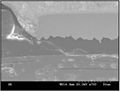
Magnified view of cross section of BGA pad and solder ball. Dielectric has cracked and the pad has started to lift, eventually creating pad cratering.
313:, PAD CRATERING: THE INVISIBLE THREAT TO THE ELECTRONICS INDUSTRY, Presented by Jim Griffin, OEM Sales & Marketing Manage, Integral Technology
164:
Solder alloy selection can impact susceptibility to pad cratering. Typically, pad cratering is considered a high strain rate event with minimal
207:
260:
396:
http://www.dfrsolutions.com/hubfs/Webinar%20Slides%20for%20YouTube/Avoiding-Pad-Cratering-and-Cracked-Capacitor-Webinar.pdf
264:
119:
255:
136:
If cratering is due to mechanical overstress then limiting board flexure is typically the best mitigation technique.
447:
275:
143:
408:
100:
28:
381:
251:
Additional information on pad cratering in printed circuit boards can be found in the following links:
322:
241:
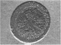
Pad crater left on printed circuit board after copper pad from a BGA connection has been pulled away.
169:
339:
173:
165:
115:
63:
419:
362:
D. Xie, D. Shangguan and H. Kroener, "Pad
Cratering Evaluation of PCB", APEX 2010, Las Vegas, NA.
147:
310:
183:
187:
47:
380:
Pad
Cratering: Assessing Long Term Reliability Risks, Denis Barbini, Ph.D., AREA Consortium,
108:
104:
51:
35:
265:
http://www.ipc.org/de/ContentPage.aspx?pageid=IPC-ehrt-Best-Papers-an-der-IPC-APEX-EXPO
436:
59:
58:, or connector insertion. However, pad cratering has also been known to occur during
423:
118:
and failure analysis such as dye and pry, acoustic emissions, cross sectioning, and
256:
http://www.smtnet.com/Forums/index.cfm?fuseaction=view_thread&Thread_ID=13953
176:
points will reduce pad cratering potential by providing additional load sharing.
214:
55:
24:
371:
31:(PCB). It may be within the resin or at the resin to fiberglass interface.
276:
http://integral-hdi.com/news/2010/11/next-generation-electronic-materials-
38:, BGA) and leaves a "crater" on the surface of the printed circuit board.
46:
Pad cratering most often occurs during dynamic mechanical events such as
20:
67:
382:
http://www.meptec.org/Resources/23%20-%20Universal%20Instruments.pdf
350:
IPC IPC-9708, Test
Methods for Characterization of PCB Pad Cratering
323:
http://www.circuitinsight.com/pdf/test_method_pad_cratering_ipc.pdf
409:"A New Approach for Early Detection of PCB Pad Cratering Failures"
70:
340:
https://www.smta.org/chapters/files/uppermidwest_padcratering.pdf
311:
https://www.smtnet.com/library/files/upload/pad-cratering.pdf
269:
172:
in the solder. More compliant solders or those with lower
182:
Board thickness and laminate material properties such as
23:
in the resin between copper foil and outermost layer of
114:
Typically, pad cratering is detected or confirmed via
34:
The pad remains connected to the component (usually a
190:(CTE) will impact susceptibility to pad cratering.
90:specifically focus on pad cratering failure modes.
407:Bansal, A.; Ramakrishna, G.; Liu, K. (2011).
8:
155:Underfill, Edge Bonding, and Corner Staking:
107:techniques such as visual inspection and
287:
278:Integral Technology pad cratering blog.
203:
168:, however there is still potential for
158:environment and application important.
335:
333:
331:
180:Board Thickness and Laminate Material:
391:
389:
358:
356:
295:
293:
291:
7:
443:Printed circuit board manufacturing
14:
234:
222:
206:
188:Coefficient of Thermal Expansion
73:selection among other factors.
94:Detection and Failure Analysis
1:
120:Scanning Electron Microscopy
464:
19:is a mechanically induced
217:exhibiting pad cratering.
50:or board flexure due to
270:http://integral-hdi.com
144:Finite Element Analysis
134:Limiting Board Flexure:
101:nondestructive testing
29:printed circuit board
200:Pad Cratering Images
146:can be done using a
272:Integral Technology
116:destructive testing
148:physics of failure
448:Soldering defects
455:
428:
427:
413:
404:
398:
393:
384:
378:
372:
369:
363:
360:
351:
348:
342:
337:
326:
320:
314:
308:
302:
297:
238:
226:
210:
109:X-Ray microscopy
105:failure analysis
56:board depaneling
48:mechanical shock
463:
462:
458:
457:
456:
454:
453:
452:
433:
432:
431:
416:Circuit Insight
411:
406:
405:
401:
394:
387:
379:
375:
370:
366:
361:
354:
349:
345:
338:
329:
321:
317:
309:
305:
298:
289:
285:
249:
242:
239:
230:
227:
218:
211:
202:
194:Board Redesign:
184:Young's modulus
128:
96:
79:
64:thermal cycling
52:In-circuit test
44:
36:Ball Grid Array
12:
11:
5:
461:
459:
451:
450:
445:
435:
434:
430:
429:
399:
385:
373:
364:
352:
343:
327:
315:
303:
286:
284:
281:
280:
279:
273:
267:
262:
258:
248:
247:External links
245:
244:
243:
240:
233:
231:
228:
221:
219:
212:
205:
201:
198:
127:
124:
95:
92:
78:
75:
43:
40:
13:
10:
9:
6:
4:
3:
2:
460:
449:
446:
444:
441:
440:
438:
425:
421:
417:
410:
403:
400:
397:
392:
390:
386:
383:
377:
374:
368:
365:
359:
357:
353:
347:
344:
341:
336:
334:
332:
328:
324:
319:
316:
312:
307:
304:
301:
296:
294:
292:
288:
282:
277:
274:
271:
268:
266:
263:
261:
259:
257:
254:
253:
252:
246:
237:
232:
225:
220:
216:
209:
204:
199:
197:
195:
191:
189:
185:
181:
177:
175:
171:
167:
163:
162:Solder Alloy:
159:
156:
152:
149:
145:
141:
137:
135:
131:
125:
123:
121:
117:
112:
110:
106:
102:
99:Conventional
93:
91:
87:
83:
76:
74:
72:
69:
65:
61:
60:thermal shock
57:
53:
49:
41:
39:
37:
32:
30:
26:
22:
18:
17:Pad cratering
415:
402:
376:
367:
346:
318:
306:
250:
213:BGA pad and
193:
192:
179:
178:
161:
160:
154:
153:
139:
138:
133:
132:
129:
113:
97:
88:
84:
80:
45:
33:
16:
15:
215:solder ball
140:Simulation:
437:Categories
283:References
170:plasticity
126:Mitigation
25:fiberglass
424:18338793
62:or even
42:Overview
21:fracture
86:modes.
77:Testing
54:(ICT),
422:
68:solder
420:S2CID
412:(PDF)
174:yield
166:creep
71:alloy
27:of a
186:and
103:and
439::
418:.
414:.
388:^
355:^
330:^
290:^
122:.
426:.
Text is available under the Creative Commons Attribution-ShareAlike License. Additional terms may apply.