1656:. The feedback loop is particularly important in non-contact AFM techniques, particularly in pc-AFM. As previously mentioned, in non-contact mode the cantilever is stationary and the tip does not come into physical contact with the sample surface. The cantilever behaves as a spring and oscillates at its resonance frequency. Topological variance causes the spring-like oscillations of the cantilever to change amplitude and phase in order to prevent the tip from colliding with sample topographies. The non-contact feedback loop is used to control that changes in the oscillations of the cantilever. The application of AFM on non-conducting samples (c-AFM) has in recent years evolved into the modification used for analysis of morphologies on the local scale, particularly morphologies at heterojunctions of multilayered samples. Photoconductive atomic force microscopy (pc-AFM) is particularly prevalent in the development of organic photovoltaic devices (OPV). The fundamental modification of c-AFM to pc-AFM is the addition of an illumination source and an inverted microscope that focuses the laser to a nanometer-scale point directly underneath the conductive AFM tip. The main concept of the illumination laser point is that it must be small enough to fit within the confines of ultra-thin films. These characteristics are achieved by using a monochromatic light source and a laser filter. In the OPV application, applying the illumination laser to the confines of ultra-thin films is further assisted by the recent development of the bulk heterojunction (BHJ) mixture of electron donating and accepting material in the film. The combination of the conductive tip and illumination laser provides photocurrent images with vertical resolutions in the range of 0 to 10 pA when overlaid with the topographical data obtained. Also unique to this modification are the spectra data gathered by comparing the current between the tip and sample to a variety of parameters including: laser wavelength, applied voltage and light intensity. The pc-AFM technique was also reported to detect local surface oxidation at a vertical resolution of 80 nm.
1826:
level and can help to increase our fundamental knowledge of mechanisms involved in OPVs at nano-scale level. pc-AFM is capable of gathering information such as the mapping of photocurrents, differences in film morphology, determination of donor-acceptor domains, current density-voltage plots, quantum efficiencies, and approximate charge carrier mobilities. One of the other notable characteristics of pc-AFM is its ability to provide concurrent information regarding the topological and photocurrent properties of the device at nano-scale. Using this concurrent sampling method, the sample handling is minimized and can provide more accurate results. In a study by
Pingree et al., pc-AFM was used to measure how spatial deviations in the photocurrent generation developed with different processing techniques. The authors were able to compare these photocurrent variations to the duration of the annealing process. They have concluded that lengthening the annealing time allows for improved nano-scale phase separation as well as created a more ordered device. Actual times for the annealing process vary depending on the properties of the polymers used. The authors have shown that external quantum efficiency (EQE) and power conversion efficiency (PCE) levels reach a maximum at certain annealing times whereas while the electron and hole mobility's do not show the corresponding trends. Therefore, while lengthening the annealing time can increase the photocurrents within the OPV, there is a practical limit to after which the benefits may not be substantial. Besides functional properties, pc-AFM can also be used to interrogate the composition heterogeneity of OPVs when combined with either Raman or infrared (IR) spectroscopy, and it is especially valuable for studying their degradation.
1882:-butyric acid methyl ester (PCBM) is explained in detail as follows. In this study, the precursor to BP (1,4:8,11:15,18:22,25-tetraethano-29H,31H-tetrabenzoporphyrin (CP) solution is applied as the starting film, and was thermally annealed which caused the CP to convert into BP. The BP:fullerene layer serves as the undoped layer within the device. For surface measurements, the undoped layer is rinsed with a few drops of chloroform and spin-dried until the BP network is exposed at the donor/acceptor interface. For bulk heterojunction characterization, an additional fullerene solution is spin-coated onto the undoped layer, a thin layer of lithium fluoride is then deposited followed by either an aluminum or gold cathode which is thermally annealed to the device. The thin layer of lithium fluoride is deposited to help prevent the oxidation of the device. Controlling the thickness of these layers plays a significant role in the generation of the efficiency of the PV cells. Typically, the thickness of the active layers is usually smaller than 100 nm to produce photocurrents. This dependence on layer thickness is due to the probability that an electron is able to travel distances on the order of exciton diffusion length within the applied electric field. Many of the organic semiconductors used in the PV devices are sensitive to water and oxygen. This is due to the likelihood of photo-oxidation which can occur when exposed to these conditions. While the top metal contact can prevent some of this, many studies are either performed in an inert atmosphere such as nitrogen, or under
2120:
damping from building supports. This source of vibrational noise is easily controlled through the use of a vibration isolation table. Acoustical vibrations are far more common than mechanical vibrations. This type of vibration is a result of air movement near the instrument such as fans or human voices. Several methods have been developed to help reduce this source of vibration. An easy solution for this is separating the electronic components from the stage. The reason for this separation of components is due to the cooling fans within the electrical devices. While operating, the fans lead to a constant source of vibrational noise within the system. In most cases, other methods still need to be employed to help reduce this source of noise. For instance, the instrument can be placed within a sealed box constructed of acoustic dampening material. Smaller stages also result in less surface area for acoustic vibrations to collide with, thus reducing the noise recorded. A more in depth solution consists of removing all sharp edges on the instrument. These sharp edges can excite resonances within the piezo-electric materials which increase the acoustic noise within the system.
1706:. The interior of the cylinder is divided into four regions (x and y regions) by non-conducting metallic strips. Electrical leads are fixed to one end and the exterior wall of the cylinder so that a current can be applied. When a voltage is applied to the exterior, the cylinder expands in x and y direction. Voltage along the interior of the tube causes cylinder expansion in the z-direction and thus movement of the tip in the z-direction. The placement of the piezo tube is dependent upon the type of AFM performed and the mode of analysis. However the z-piezo must always be fixed above the tip and cantilever to control the z-motion. This configuration is most often seen in the c-AFM and pc-AFM modifications to make room for additional instrumental components which are placed below the scanning stage. This is particularly true for pc-AFM, which must have the piezo-components arranged above the cantilever and tip so that the illumination laser can transmit through the sample.with applied voltage
233:. Conductive AFM has been widely used in characterizing the local electric properties in both photovoltaic fullerene blends and organic films, but no reports have shown the use of c-AFM to display the distribution of photocurrents in organic thin films. The most recent variation of SPM devices include (tr-EFM) and photoconductive AFM (pc-AFM) . Both these techniques are capable of obtaining information regarding photo-induced charging rates with nano-scale resolution. The advantage of pc-AFM over tr-ERM is present in the maximum obtainable resolution by each method. pc-AFM can map photocurrent distributions with approximately 20 nm resolution, whereas tr-EFM was only able to obtain between 50 and 100 nm resolution at this time. Another important factor to note is although the tr-EFM is capable of characterizing thin films within organic solar cells, it is unable to provide the needed information regarding the capacitance gradient nor the surface potential of the thin film.
1942:
mode is less destructive to the sample, but the tip is more likely to drift out of contact with the surface and thus it may not record data. Drifting of the tip is also seen due to piezo hysteresis, which causes displacement due to molecular friction and polarization effects due to the applied electric field. It is important to note the correlation between resolution and curvature of tip radius. Early STM tips used by
Binning and Rohrer were fairly large, anywhere between some hundred nm to 1 μm in radius. In more recent work, the tip radius of curvature was mentioned as 10–40 nm. By reducing the radius of curvature of the tip, it allows for the enhanced detection of deviations within the OPVs surface morphology. Tips often need to be replaced due to tip rounding, which leads to a decrease in the resolution. Tip rounding occurs due to the loss of outermost atoms present at the apex of the tip which can be a result of excessive force applied or character of the sample.
1793:
the photocurrents are mapped in this direction. Therefore, normal AFM/c-AFM can be implemented for analysis in the x and y directions. The instrumental module proposed by Lee et al. produced spot sizes from the illumination laser of 1 mm in thicknesses. Recent applications have altered Lee's design in order to decrease spot size while simultaneously increasing the intensity of this laser. Recent instrumentation has replaced the angled mirror with an inverted microscope and a neutral density filter. In this device the x and y piezos, illumination laser and inverted microscopy are confined underneath the sample substrate, while the z-piezo remains above the conductive cantilever. In the applications of Ginger et al. a neutral-density filter is added to increase laser attenuation and the precision of laser alignment is enhanced by the addition of the inverted microscope.
1862:, is a transparent, polymeric conductive layer which is usually placed between the ITO and the active OPV layer. The PEDOT:PSS is a conductive polymer is stable over various applied charges. In most studies, PEDOT:PSS is spin-coated onto the ITO-coated glass substrates directly after plasma cleaning of the ITO. Plasma cleaning, as well as halo-acid etching, have been shown to improve the surface uniformity and conductivity of the substrate. This PEDOT:PSS layer is then annealed to the ITO prior to spin-coating the OPV layer onto the substrate. Studies by Pingree et al. have shown the direct correlation between annealing time and both peak and average photocurrent generation. Once this OPV film is spin-coated onto the substrate, it is then annealed at temperatures between 70 and 170 °C, for periods up to an hour depending on the procedure as well as OPV being used.
1047:
piezo-tube becomes displaced by an angle, θ. As the tube is displaced, the sample that, in traditional AFM is fixed to the tube generates lateral translation and rotation relative to the AFM tip, thus movement of the tip is generated in the x and y directions When voltage is applied of the inside of the tube, movement in the z-direction is implemented. The relationship between the movement of the piezo-tube and the direction of the displacement of the AFM tip assumes that the tube is perfectly symmetric. When no voltage is applied to the tube the z-axis bisects the tube, sample and sample stage symmetrically. When a voltage is applied to the exterior of the tube (x and y motion), the expansion of the tube can be understood as a circular arc. In this equation, the
1735:
traditional AFM their configuration is tailored to measuring surface currents on the local scale. As mentioned previously, the piezo-tube can be placed either above or below the sample, depending on the application of the instrumentation. In the case of c-AFM, repulsive contact mode is the predominantly used to obtain electric current images from the surface as the sample moves in the x and y direction. Placing the z-piezo above the cantilever allows for better control of the cantilever and tip during analysis. The material that comprises the conductive tip and cantilever can be customized for a particular application. Metal-coated cantilevers, gold wires, all-metal cantilevers and
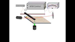
58:. This property is largely attributed to resistance that is characteristic of the organic layer. The fundamentals of pc-AFM are modifications to traditional AFM and focus on the use of pc-AFM in PV characterization. In pc-AFM the major modifications include: a second illumination laser, an inverted microscope and a neutral density filter. These components assist in the precise alignment of the illumination laser and the AFM tip within the sample. Such modifications must complement the existing principals and instrumental modules of pc-AFM so as to minimize the effect of mechanical noise and other interferences on the cantilever and sample.
1971:
to determine the impact the illumination process exhibits on the OPV. Short circuit measurements are also commonly performed on the OPV devices. This consists of engaging the illumination source at open current (that is applied potential to the sample is zero). Nguyen and workers noted that a positive photocurrent reading correlated to the conduction of holes, while a negative reading correlated to the conduction of electrons. This alone allowed the authors to make predictions regarding the morphology within the cell. The current density for the forward and reverse bias can calculated as follows:
637:
sample while simultaneously measuring changes in the topographical features. In all techniques of AFM, two modes of operation can be used: contact mode and non-contact mode. In c-AFM resonant contact mode is used to obtain topographical from current that is measured between the biased AFM tip and the sample surface. In this type of operation, the current is measured in the small space between the tip and the sample surface. This quantification is based on the relationship between the current traveling through the sample and layer thickness. In the previous equation, A
1026:
258:
largely dependent on the fundamentals of the AFM cantilever, metallic tip, scanning piezo-tube and the feedback loop that transfers information from lasers that guide the motion of the probe across the surface of a sample. The ultra-fine dimensions of the tip and the way the tip scans the surface produces lateral resolutions of 500 nm or less. In AFM, the cantilever and tip functions as a mass on a spring. When a force acts on the spring (cantilever), the spring response is directly related to the magnitude of the force.
194:, and phase-separated domains. Many of these problems arise from the deficient knowledge of electro-optical properties on the nano-scale level. In numerous studies, it has been observed that heterogeneities in the electrical and optical properties influence device performance. These heterogeneities which occur in OPVs are a result the manufacturing process, such as annealing time, which is explained below. Research has mainly consisted of discovering exactly how this film morphology affects the device performance.
1765:
between the illumination laser and the guiding laser was also a concern. First attempts to address these two issues was to place a prism between the sample tip and the surface such that the prism would allow the illumination laser to reflect at the interface between the prism and the laser and thus be focused to a localized spot on the sample surface. However, lack of space for the prism and the production of multiple light reflections when introducing a prism required a different concept for configuration.
1756:
modified from existing cp-AFM instrumentation. The first report of this instrumental modification came in 2008. In that paper, Lee and coworkers implemented the aforementioned modifications to examine the resolution of photocurrent imaging. Their design consisted of three main units: a conductive mirror plate, steering mirror and laser source. The main difficulty with the previously existing c-AFM instrumentation is the inability of the technique for characterizing
685:
1710:
to the piezo corresponding to the appropriate direction of tip displacement. In this type of set-up the sample and substrate are mounted on top of the z-piezo component. When the x and y piezo components are in use, the orthogonal design causes them to push against the base of the z-piezo, causing the z-piezo to rotate about a fixed point. Applying voltage to the z-piezo causes the tube to move up and down on its pivot point.
156:). This global demand for solar energy increased 54% in 2010, while the United States alone has installed more than 2.3 GW of solar energy sources in 2010. Some of the attributes which make OPVs such a promising candidate to solve this problem include their low-cost of production, throughput, ruggedness, and their chemically tunable electric properties along with significant reduction in the production of
1021:{\displaystyle I=A_{\text{eff}}\left({\frac {q^{2}m_{o}}{8\pi hm_{\text{eff}}}}\right)\left({\frac {1}{t\left(E^{2}\right)}}\right)\left({\frac {\beta ^{2}V^{2}}{\phi d^{2}}}\right)e^{\left(\left({\frac {\left(8\pi \right)\left(2m_{\text{eff}}q\right)^{\frac {1}{2}}}{\left(3h\right)}}\right)\left(\nu \left(E\right)\right)\left({\frac {d}{\beta V}}\right)\left(\phi ^{\frac {1}{3}}\right)\right)}}
2103:
464:. There is also a force exerted from the cantilever pressing down on the tip. The magnitude of the force exerted by the cantilever is dependent upon the direction of its motion, whether it is attracted or repelled from the sample surface When the tip of the cantilever and the surface come into contact, the single atom at the point of the tip and the atoms on the surface exhibit a
5147:
2094:
1841:(InAs) quantum dots through the implementation of pc-AFM. Through the use of pc-AFM, information regarding quantum dot size, as well as the dispersion of quantum dots within the device, can be recorded in a non-destructive manner. This information can then be used to display local variances in photoactivity relating to heterogeneities within the film morphology.
1866:
1769:
employed as a means of controlling the trajectory of the laser source, with this addition the position of the reflected beam on the sample could be easily adjusted for placement underneath the AFM tip. The illumination laser source was a diode-pumped solid-state laser system that produced a wavelength of 532 nm and a spot of 1 mm in the sample.
1898:
1934:
1660:
1926:. As the sampling begins, the tip is moved close to the sample which creates a weakly attractive force between them. Another force which is often present in contact mode is capillary force due to hydration on the sample surface. This force is due to the ability of the water to contact the tip, thus creating an undesirable attractive force.
209:(STXM). These methods are very useful in the identification of the local morphology on the film surface, but lack the ability to provide fundamental information regarding local photocurrent generation and ultimately on the device performance. To obtain information which links the electrical and optical properties, the use of electrical
1714:
1748:
1691:
20:
1813:
1031:
manufactured as a cylinder. In all techniques, sample topography is measured by the movement of the x and y piezos. When performing non-contact mode pc-AFM, the piezo-tube keeps the probe from moving in the x and y direction and measures the photocurrent between the sample surface and conducting tip in the z-direction.
1922:
detector. The z-piezo scanner then recognizes this deviation and moves vertically to return the laser spot to its set position. This vertical movement by the z-piezo scanner is correlated to a change in voltage. Sampling in contact mode relies upon intermolecular forces between the tip and surface as depicted by
2116:
experience attractive forces between them. This current density measurement is then combined with the topographical information previously gathered from the AFM tip and cantilever. The resulting image displays the local variations in morphology with the current density measurements superimposed onto of them.
2115:
to the sample through the spotted gold contact. By adjusting this bias, along with the current passing through the cantilever, one can adjust the repulsive/attractive forces between the sample and the tip. When a reverse bias is applied (tip is negative relative to the sample), the tip and the sample
1970:
images of the sample. Dark current is referred to as the photocurrent generation created by the OPV in the absence of an illumination source. The cantilever and tip are simply rastered across the sample while topographic and current measurements are obtained. This data can then be used as a reference
1917:
Once the sample preparation is complete, the sample is placed onto the scanning stage of the pc-AFM module. This scanning stage is used for x-y piezo translation, completely independent of the z-direction while using a z-piezo scanner. The piezo-electric material within this scanner converts a change
1808:
which carries relatively small current within it, is able to generate nano-scale holes within the sample material to which the two electrodes are able to detect the relatively small change in conductance due to the flow from the top electrode to the bottom electrode. The combination of these elements
1792:
The conductive AFM tip was easily aligned over the reflected illumination beam. The laser spot in the sample was reported to be 1mm in size and can be found using the AFM recording device. A convenience of this technique is that laser alignment is only necessary for imaging in the z-direction because
1781:
images that were taken with and without the placement of the mirror and laser. This particular set-up required the separation of the x, y and z piezo-scanners The separation of piezo-tubes accounts for the elimination of x-z cross-coupling and scanning-size errors, which is common in traditional AFM.
1681:
that is positioned adjacent to the illumination source. The technical parameters of pc-AFM are identical to those of traditional AFM techniques. This section will focus on the instrumentation necessary for AFM and then detail the requirements for pc-AFM modification. The main instrumental components
2097:
Unannealed film: (a) current-voltage plot under 632 nm laser with platinum AFM tip, (b) pc-AFM under short circuit representation, and (c) dark current-voltage plots. Annealed film: (d) illuminated current-voltage characteristics, (e) pc-AFM short circuit representation, and (f) dark current-voltage
1764:
The first main concern deals with component configuration and whether or not there is physically enough space for modification in the cramped c-AFM module. The component configuration must be such the addition of the laser illumination component does not cause disturbance to other units. Interaction
1755:
The main components and instrumentation of c-AFM instrumentation are identical to that required for a pc-AFM module. The only modifications are the illumination source, filter and inverted microscope objective that are located beneath the sample substrate. In fact, most pc-AFM instruments are simply
1743:
in ambient conditions. The main difference between the instrumentation of c-AFM and STM is that in c-AFM the bias voltage can be directly applied to the nanostructure (tip and substrate). In STM, on the other hand, the applied voltage must be supported within the vacuum tunneling gap between the STM
1709:
In some configurations, the piezo components can be arranged in a tripod design. In this type of set-up, the x, y and z components are arranged orthogonally to one another with their apex attached to a movable pivot point. Similar to the cylindrical piezo, in the tripod design the voltage is applied
257:
The fundamental principles of photoconductive atomic force microscopy (pc-AFM) are based on those of traditional atomic force microscopy (AFM) in that an ultrafine metallic tip scans the surface of a material to quantify topological features. The working premises for all types of AFM techniques are
164:
PV device, which ultimately yielded a power conversion efficiency of 1%. Tang's research was published in 1986, which allowed others to decipher many of the problems which limited the basic understanding of the process involved in the OPVs. In later years, the majority of the research focused on the
2119:
Several methods have been employed to help reduce both mechanical and acoustic vibrations within the system. Mechanical vibrations are mainly attributed to traffic in and out of a building Other sources of mechanical vibrations have often been seen in the higher stories of a building due to reduced
1954:
have also been widely used as illumination sources, but are atypical in recent work. In a study by Coffey et al., lasers of two different wavelengths (532 nm and 405 nm) are irradiated onto the same sample area. With this work, they have shown images with identical contrast which proves
1941:
There are considerations which need to be taken into account when determining which mode is optimal for sampling for a given application. It has been shown that sampling in contact mode with very soft samples can damage the sample and render it useless for further studies. Sampling in non-contact
1825:
Although there is significant insight as to how OPVs work, it is still difficult to relate the device's functionality to local film structures. This difficulty may be attributed to the minimal current generation at a given point within OPVs. Through pc-AFM, OPV devices can be probed at nano-scale
1780:
The addition of the mirror and laser underneath the sample substrate results in a higher scanning level due to raising the sample substrate. This configuration has no effect on any other instrument component and does not affect AFM performance. This result was confirmed by identical topographical
1784:
In addition there was no evidence of laser interferences between the guiding laser and the irradiation laser. The guiding laser, at a wavelength of 650 nm, hits the mirror on the back of the conducting cantilever from vertical trajectory and is reflected away from the cantilever towards the
1768:
The module constructed by Lee et al. implemented a tilted mirror plate that was positioned underneath the sample substrate. This conductive mirror was tilted at 45° and successfully reflected the illuminating laser to a focused spot directly underneath the conductive tip. The steering mirror was
1760:
devices. Specifically, it is difficult to measure changes in local and nano-scale electrical properties that result from the photonic effect. The optical illumination component (laser) was added to the c-AFM module in order to make such properties visible. Early in development, the main concerns
636:
Modifications of this early work have been implemented to perform AFM analysis on both conducting and non-conducting materials. Conductive atomic force microscopy (c-AFM) is one such modification technique. The c-AFM technique operates by measuring fluctuations in current from the biased tip and
1945:
Because of the extremely small radius of the AFM tip, the illumination source is allowed to be focused tighter, thus increasing its efficiency. Typical arrangements for pc-AFM contain a low powered, 532 nm laser (2–5 mW) whose beam is reflected off mirrors located beneath the scanning
1046:
material reacts with an applied voltage to either the interior or exterior of the tube. When voltage is applied to the two electrodes connected to the scanner, the tube will expand or contract causing motion to the AFM tip in the direction of this movement. This phenomenon is illustrated as the
189:
as compared to other high efficiency polymers. These copolymers have been widely researched due to their ability to be tuned for specific optical and electrical properties. To date, the best OPV devices have a maximum power conversion efficiency of approximately 8.13%. This low power conversion
1906:
1686:
components and the sample substrate. The components for photoconductive modification include: the illumination source (532 nm laser), filter and inverted microscope. When modifying traditional AFM for pc application, all components must be combined such that they do not interfere with one
1921:
Many commercial AFM cantilever tips have pre-measured resonant frequencies and force constants which are provided to the customer. As sampling proceeds, the cantilever tip's position changes, which causes the scanning laser wavelength (650 nm) to deviate from its original position on the
1030:
The accuracies of all AFM techniques rely heavily on a sample scanning tube, the piezo-tube. The piezo-tube scanner is responsible for the direction of tip displacement during a sample analysis, and is dependent on the mode of analysis. The piezo components are either arranged orthogonally or
1734:
The instrumentation of conductive AFM (c-AFM) has evolved with the desire to measure local electrical properties of materials with high resolutions. The essential components are: the piezo-tube, the guide laser, the conducting tip, and cantilever. Although these components are identical to
1726:
is focused through the tube and onto a mirror that rests on tip of the cantilever. The guiding laser is reflected off of the mirror and detected by a photodetector. The laser senses when the forces acting on the tip change. The reflected laser beam from this phenomenon reaches the
248:
in physics in 1986. They fabricated an instrument called scanning tunneling microscope (STM) and demonstrated that STM provides surface topography on the atomic scale. This microscopy technique yielded resolutions which were nearly equal to scanning electron microscopy (SEM).
1858:(ZnO) and carbon nanotubes as an alternative to ITO. Although these semiconductors are relatively inexpensive, high quality ITO layers are still being used extensively for PV applications. Poly(3,4-ethylenedioxythiophene) poly(styrenesulfonate), more commonly known as
460:. Attractive forces between the atoms on the sample surface and the atom at the AFM tip draw the cantilever tip closer to the surface. When the cantilever tip and the sample surface come within a range of a few angstroms repulsive forces come into play as a result of
4559:
Westenhoff, S.; Howard, Ian A.; Hodgkiss, Justin M.; Kirov, Kiril R.; Bronstein, Hugo A.; Williams, Charlotte K.; Greenham, Neil C.; Friend, Richard H.; et al. (2008). "Charge
Recombination in Organic Photovoltaic Devices with High Open-Circuit Voltages".
1672:
The instrumentation involved for pc-AFM is very similar to that necessary for traditional AFM or the modified conductive AFM. The main difference between pc-AFM and other types of AFM instruments is the illumination source that is focused through the inverted
1648:
81:, in which photoconductivity was observed. Anthracene was heavily studied due to its known crystal structure and its commercial availability in high-purity single anthracene crystals. The studies of photoconductive properties of organic dyes such as
1744:
probe and surface. When the tip is in close contact with the sample surface the application of bias voltage to the tip creates a vacuum gap between the tip and the sample that enables the investigation of electron transport through nanostructures.
1849:
Sample preparation of the OPV is of the utmost importance when performing pc-AFM studies. The sampling substrate is recommended to be conductive, as well as transparent, to the light source which is irradiated upon it. Numerous studies have used
1789:(PSPD). The illumination beam, on the other hand, travels from underneath the sample platform and is reflected into position by the reflecting mirror. The angle of the mirror plate ensures that the beam does not extend past the sample surface.
1773:
2106:
a) Superimposed photocurrent map and three-dimensional film topography collected from a conductive AFM tip (diamond coated) while under short circuit conditions. (b) Reduced scan area which depict local current-voltage measurements in
632:
2056:
190:
efficiency is directly related to discrepancies in the film morphology on the nano-scale level. Explanations of film morphology include recombination and/or trapping of charges, low open circuit voltages, heterogeneous interfaces,
1918:
in the applied potential into mechanical motion which moves the samples with nanometer resolution and accuracy. There are two variations in which the z-piezo scanner functions; one is contact mode while the other is tapping mode.
1959:
1504:
4832:
Li, Jiangyu; Huang, Boyuan; Esfahani, Ehsan Nasr; Wei, Linlin; Yao, Jianjun; Zhao, Jinjin; Chen, Wei (2017). "Touching is believing: interrogating halide perovskite solar cells at the nanoscale via scanning probe microscopy".
1761:
regarding pc-AFM include: physical configuration, laser disturbance and laser alignment. Although many of these concerns have been resolved pc-AFM modules are still widely modified from c-AFM and traditional AFM instruments.
1370:
1035:
4598:
X.-D. Dang; A.B. Tamayo; J. Seo; C.V. Hoven; B. Walker; T.-Q. Nguyen (2010). "Nanostructure and
Optoelectronic Characterization of Small Molecule Bulk Heterojunction Solar Cells by Photoconductive Atomic Force Microscopy".
1721:
The other essential components of AFM instrumentation include the AFM tip module, which includes: the AFM tip, the cantilever, and the guiding laser. When the piezo-tube is positioned above the cantilever and tip, the
1702:. Most cylindrical piezos are between 12 and 24 mm in length and 6 and 12 mm in diameter. The exterior of the piezo-tube is coated with a thin layer of conducting metal so that this region can sustain an
1277:
4661:
C.V. Hoven; X.-D. Dang; R.C. Coffin; J. Peet; T.-Q. Nguyen; G.C. Bazan (2010). "Improved
Performance of Polymer Bulk Heterojunction Solar Cells Through the Reduction of Phase Separation via Solvent Additives".
3550:
H. J. Lee; S. M. Park (2004). "Electrochemistry of
Conductive Polymers. 30. Nanoscale Measurements of Doping Distributions and Current−Voltage Characteristics of Electrochemically Deposited Polypyrrole Films".
440:
3501:
H.-N. Lin; H.-L. Lin; S.-S. Wang; L.-S. Yu; G.-Y. Perng; S.-A. Chen; S.-H. Chen (2002). "Nanoscale charge transport in an electroluminescent polymer investigated by conducting atomic force microscopy".
4903:
Madl, M.; Brezna, W.; Strasser, G.; Klang, P.; Andrews, A. M.; Bodnarchuk, M. I.; Kovalenko, M. V.; Yarema, M.; Heiss, W. (2011-01-10). "AFM-based photocurrent imaging of epitaxial and colloidal QDs".
4505:
Madl, M.; Brezna, W.; Klang, P.; Andrews, A. M.; Strasser, G.; Smoliner, J. (2010). "High resolution photocurrent imaging by atomic force microscopy on the example of single buried InAs quantum dots".
4797:
O. Douheret; L. Lutsen; A. Swinnen; M. Breselge; K. Vandewal; L. Goris; J. Manca (2006). "Nanoscale electrical characterization of organic photovoltaic blends by conductive atomic force microscopy".
1809:
produced laser intensities in the range of 10 to 108 W/m and decreased the size of the laser spot to sub-micrometer dimensions making this technique useful for the application of nm thin OPV films.
1189:
1134:
3171:
Cornil, D. Beljonne, J. P. Calbert, J. L. Bredas (2001). "Interchain
Interactions in Organic π-Conjugated Materials: Impact on Electronic Structure, Optical Response, and Charge Transport".
4196:
Dante, M., Peet, J., Nguyen, T.Q. (2008). "Nanoscale Charge
Transport and Internal Structure of Bulk Heterojunction Conjugated Polymer/Fullerene Solar Cells by Scanning Probe Microscopy".
2820:
L.S.C. Pingree; O.G. Reid; D.S. Ginger (2010). "Imaging the
Evolution of Nanoscale Photocurrent Collection and Transport Networks during Annealing of Polythiophene/Fullerene Solar Cells".
2650:
H. Xin; O.G. Reid; G. Ren; F.S. Kim; D.S. Ginger; S.A. Jenekhe (2010). "Polymer nanowire/fullerene bulk heterojunction solar cells: How nanostructure determines photovoltaic properties".
2958:
D.C. Coffey; O.G. Reid; D.B. Rodovsky; G.P. Bartholomew; D.S. Ginger (2007). "Mapping Local
Photocurrents in Polymer/Fullerene Solar Cells with Photoconductive Atomic Force Microscopy".
1510:
1731:. The output from this detector acts as a response to the changes in force and the cantilever adjusts the position of the tip, while keeping constant the force that acts on the tip.
144:(OPV) devices (organic solar cells), have been studied extensively to help in reducing the dependence on fossil fuel and containing the emission of green house gases (especially CO
85:
were initiated only in the early 1960s owing to the discovery of the PV effect in these dyes. In further studies, it was determined that important biological molecules such as
5338:
5074:
160:. For decades, the researchers have believed that the maximum power conversion efficiency (PCE) would most likely remain below 0.1%. Only in 1979 Tang reported a two-layer,
4634:
M. Dante; A. Garcia; T.-Q. Nguyen (2010). "Three-Dimensional Nanoscale Organization of Highly Efficient Low Band-Gap Conjugated Polymer Bulk Heterojunction Solar Cells".
4146:
Groves, C.; et al. (2010). "Heterogeneity in polymer solar cells: local morphology and performance in organic photovoltaics studied with scanning probe microscopy".
2870:
M. Guide; X.D. Dang; T.Q. Nguyen (2011). "Nanoscale Characterization of Tetrabenzoporphyrin and Fullerene-Based Solar Cells by Photoconductive Atomic Force Microscopy".
2702:
T.A. Bull; L.S.C. Pingree; S.A. Jenekhe; D.S. Ginger; C.K. Luscombe (2010). "The Role of Mesoscopic PCBM Crystallites in Solvent Vapor Annealed Copolymer Solar Cells".
4223:
4071:
3929:
3816:
3678:
3417:
3198:
54:(PV) devices between two electrodes, in which PV properties rely heavily on the nature of the electrodes. In addition, single layer PV devices notoriously have a poor
3474:
L. S. C. Pingree; B. A. Macleod; D. S. Ginger (2008). "The Changing Face of PEDOT:PSS Films: Substrate, Bias, and Processing Effects on Vertical Charge Transport".
302:
185:
donor-acceptor copolymers have been created for PCBM-based OPV devices. These low band-gap donor-acceptor copolymers are able to absorb a higher percentage of the
489:
5129:
4379:
Tanaka, I.; et al. (1999). "Imaging and probing electronic properties of self-assembled InAs quantum dots by atomic force microscopy with conductive tip".
3431:
C. Ionescu-Zanetti; A. Mechler; S. A. Carter; R. Lal (2004). "Semiconductive Polymer Blends: Correlating Structure with Transport Properties at the Nanoscale".
1981:
4414:
Wold, D.J.; et al. (2000). "Formation of Metal−Molecule−Metal Tunnel Junctions: Microcontacts to Alkanethiol Monolayers with a Conducting AFM Tip".
4754:
O.G. Reid; K Munechika; D.S. Ginger (2008). "Space Charge Limited Current Measurements on Conjugated Polymer Films using Conductive Atomic Force Microscopy".
2090:
is the film thickness in nanometers. The majority of the organic materials have relative permeability values of ~3 in their amorphous and crystalline states.
1663:
Photocurrent resolutions compared with a traditional topographical image. Reproduction granted by The American Chemical Society. License Number: 2656610690457
5134:
4090:
Sakaguchi, H.; et al. (1999). "Nanometer-Scale Photoelectric Property of Organic Thin Films Investigated by a Photoconductive Atomic Force Microscope".
3614:
1854:-coated glass as their conductive substrate. Because of high cost of ITO, however, there have been attempts to utilize other semiconducting layers, such as
1388:
306:
The forces acting on the tip are such that the spring (cantilever) remains soft but responds to the applied force, with a detectable resonant frequency,
1739:
cantilevers are used. In many cases diamond is the preferred material for cantilever and/or tip because it is an extremely hard material that does not
1292:
3368:
A. M. Nardes, M. Kemerink, R. A. J. Janssen, J. A. M. Bastiaansen, N. M. M. Kiggen, B. M. W. Langeveld, A. J. J. M. van Breemen, M. M. de Kok (2007).
3293:
Jaquith, Michael; Muller, Erik M.; Marohn, John A. (2007). "Time-Resolved Electric Force Microscopy of Charge Trapping in Polycrystalline Pentacene".
353:
must also decrease to increase the value of the ratio. Manipulating the values in this way provides the necessary high resonance frequency. A typical
4957:
M. Taub; B. Menzel; G. Khanna; E. Lilleodden (2003). SPM Training Manual, Vers. 2.0 (Report). Laboratory for Advanced Materials, Stanford University.
2750:
B.H. Hamadani; S. Jung; P.M. Haney; L.J. Richter; N.B. Zhitenev (2010). "Origin of Nanoscale Variations in Photoresponse of an Organic Solar Cell".
2545:
2111:
The range of bias commonly applied is usually limited to between −5 V to +5 V for most studies. This can be achieved by applying a forward bias or
5067:
1833:. Because if their relative ease of use, along with size-tunable excitation attributes, quantum dots have commonly been applied as sensitizers in
3341:
Kemerink, M.; Timpanaro, S.; De Kok, M. M.; Meulenkamp, E. A.; Touwslager, F. J. (2004). "Three-Dimensional Inhomogeneities in PEDOT:PSS Films".
5194:
5164:
5022:
4994:
4715:"Measurement of nanoscale external quantum efficiency of conjugated polymer:fullerene solar cells by photoconductive atomic force microscopy"
3913:
3800:
1200:
1890:
1910:
170:
5246:
5241:
5226:
5189:
5112:
381:
5359:
5102:
5060:
226:
2276:"Die verschiedenen lichtelektrischen Erscheinungen am Anthracen, ihre Beziehungen zueinander, zur Fluoreszenz und Dianthracenbildung"
324:
is defined as the mass acting on the cantilever: the mass of the cantilever itself and the mass of the tip. The relationship between
50:
Multi-layer photovoltaic cells have gained popularity since mid 1980s. At the time, research was primarily focused on single-layer
4265:
3184:
202:
1694:
Schematic of AFM sample analysis components. Reproduction granted by The American Chemical Society. License Number: 265674124703
5364:
5256:
5221:
3212:
E. Moons (2002). "Conjugated polymer blends: linking film morphology to performance of light emitting diodes and photodiodes".
4470:
Lee, J.; et al. (2008). "Construction of pcAFM module to measure photoconductance with a nano-scale spatial resolution".
5374:
5369:
5236:
5216:
5211:
5174:
3952:
Olbrich, A.; et al. (1998). "Conducting atomic force microscopy for nanoscale electrical characterization of thin SiO".
3001:
A. Sharma; G. Andersson; D.A. Lewis. (2011). "Role of humidity on indium and tin migration in organic photovoltaic devices".
1930:, along with several other sources of tip contamination, are key factors in the decreased resolution observed while sampling
214:
130:
2604:
L.S.C. Pingree; O.G. Reid; D.S. Ginger (2010). "Electrical Scanning Probe Microscopy on Active Organic Electronic Devices".
456:. Changes in these forces are monitored by a guide laser that is reflected off the back of the cantilever and detected by a
5179:
5124:
2129:
1071:, is expressed as the intensity of the electric field applied to the exterior of the tube, the voltage along the x-axis, U
222:
218:
4053:
1829:
In more recent studies, pc-AFM has been employed to gather information regarding the photoactive regions from the use of
1140:
1085:
105:
which are slightly more expensive than organic based solar cells. The commonly used inorganic based solar cells include
101:
also exhibited the PV effect. Although many different blends have been researched, the market is dominated by inorganic
5276:
5271:
2222:
A. E. Becquerel (1839). "Research on the effects of chemical radiation from sunlight by means of electric currents".
468:. The atoms exhibit attractive forces until a certain point and then experience repulsion from one another. The term
3578:
K. D. O'Neil; B. Shaw; O. A. Semenikhin (2007). "On the Origin of Mesoscopic Inhomogeneity of Conducting Polymers".
2348:"The crystal and molecular structure of anthracene. II. Structure investigation by the triple Fourier series method"
1796:
One of the most common pc-AFM setups incorporates a light source, which emits in the visible spectrum along with an
1643:{\displaystyle dz=\left(\left(R+\chi \right)sin\Theta -L\right)+\left(D_{ss}+D_{sp}\right)\left(cos\Theta -1\right)}
5292:
5206:
5146:
2390:
G.J. Sloan (1966). "Studies on the Purification of Anthracene; Determination and Use of Segregation Coefficients".
461:
5302:
5266:
5261:
5184:
5169:
5083:
3618:
210:
177:, dictated the majority of studies pertaining to OPV for many years. In more recent research, polymer-based bulk
5037:
AFM Instrumentation. AFM University, Atomic Force Microscopy Education Resource Library. Web. 21 Apr. 2011. <
1687:
another and so that various sources of noise and mechanical interference do not disrupt the optical components.
5231:
2195:
H. Spanggaard; F.C. Krebs (2004). "A brief history of the development of organic and polymeric photovoltaics".
55:
5297:
5097:
480:
465:
453:
198:
35:
5041:
1698:
In traditional instrumentation, the stage is a cylindrical piezo-tube scanner that minimizes the effect of
1967:
1678:
5251:
4217:
3672:
3411:
3192:
3144:
Hoppe, H.; Sariciftci, N. S. (2006). "Morphology of Polymer/Fullerene Bulk Heterojunction Solar Cells".
2549:
1947:
230:
2444:
G.J. Sloan; J.M. Thomas; J.O. Williams (1975). "Basal Dislocations in Single Crystals of Anthracene".
4912:
4852:
4806:
4763:
4726:
4671:
4514:
4388:
4348:
4339:
O’Shea, S.J.; et al. (1995). "Characterization of tips for conducting atomic force microscopy".
4296:
4099:
3961:
3861:
3650:
3511:
3440:
3381:
3221:
3110:
3010:
2967:
2879:
2829:
2759:
2453:
2426:
2399:
2359:
2326:
2287:
2160:
1804:). The use of a gold plated silicon AFM probe is often used as the top anode in pc-AFM studies. This
1674:
449:
141:
122:
1923:
1699:
1067:
is the extension of the tube after the voltage is applied. The change in length of the piezo-tube,
51:
221:(SKPM) have been utilized in the studies of electron injection and charge trapping effects, while
4876:
4842:
4695:
4616:
4538:
4115:
3923:
3810:
3456:
3399:
3237:
3126:
2903:
2621:
372:
5018:
4990:
4928:
4868:
4779:
4687:
4577:
4530:
4487:
4326:
Materials Evaluation and Engineering Inc. Handbook of Analytical Methods For Materials. (2009)
4163:
4065:
3909:
3879:
3796:
3595:
3310:
3026:
2983:
2895:
2845:
2775:
2719:
2667:
1883:
1837:
devices. The authors have studied the photoresponse of sub-surface foundations such as buried
134:
69:
after illumination when he submerged platinum electrodes within an aqueous solution of either
39:
5307:
4920:
4860:
4814:
4771:
4734:
4679:
4643:
4608:
4569:
4522:
4479:
4423:
4396:
4356:
4304:
4205:
4155:
4107:
4015:
3969:
3869:
3658:
3587:
3560:
3519:
3483:
3448:
3389:
3350:
3302:
3273:
3229:
3180:
3153:
3118:
3071:
3018:
2975:
2887:
2837:
2767:
2711:
2659:
2613:
2526:
2461:
2434:
2407:
2367:
2334:
2295:
2204:
2168:
1851:
1797:
1683:
627:{\displaystyle f={-\mathrm {d} V \over \mathrm {d} r}={24\varepsilon _{o} \over r_{o}}\left}
206:
191:
157:
126:
3056:
275:
197:
Until recently, microscopy methods used in the characterization of these OPVs consisted of
5045:
2051:{\displaystyle J={\frac {8}{9}}\varepsilon _{o}\varepsilon _{r}\mu {\frac {V^{3}}{L^{3}}}}
1927:
1838:
241:
110:
70:
62:
1901:
Chemical structure of (1,4:8,11:15,18:22,25-tetraethano-29H,31H-tetrabenzoporphyrin (CP).
4916:
4856:
4810:
4767:
4730:
4675:
4526:
4518:
4392:
4352:
4300:
4103:
3965:
3865:
3654:
3515:
3444:
3385:
3225:
3114:
3014:
2971:
2883:
2833:
2763:
2457:
2430:
2403:
2363:
2330:
2291:
2164:
5323:
4269:
2481:
1951:
1834:
1703:
1043:
675:, the field enhancement factor, accounts for the non-planar, geometry of the tip used.
266:
186:
178:
98:
82:
77:. In the early 20th century, Pochettino and Volmer studied the first organic compound,
74:
3615:
New Scanning Probe Techniques for Analyzing Organic Photovoltaic Materials and Devices
3278:
3261:
3233:
1878:
A recently developed OPV system based on tetrabenzoporphryin (BP) and either -phenyl-C
663:= 0.5, which is the effective mass of an electron in the conduction band of a sample,
5353:
4699:
4620:
4119:
3460:
3403:
3241:
2625:
2530:
1786:
1653:
1499:{\displaystyle dx=(R+\chi )\left(1-cos\Theta \right)+\left(D_{ss}+D_{sp}\right)U_{x}}
457:
61:
The original exploration of the PV effect can be accredited to research published by
4880:
4542:
3130:
3095:
2907:
2233:
A.E. Becquerel (1839). "On Electrod Effect under the Influence of Solar Radiation".
475:
is the separation at which the sum of the potentials between the two atoms is zero
4483:
4285:"Noninvasive determination of optical lever sensitivity in atomic force microscopy"
4245:
Geisse, N. AFM and combined optical techniques. Application Note 12 Asylum research
4019:
3370:"Microscopic Understanding of the Anisotropic Conductivity of PEDOT:PSS Thin Films"
2112:
1955:
that the photocurrent variations are less related to spatial absorbance variation.
1889:
1830:
86:
66:
2102:
1869:
Deviation of the laser spot on photo diode caused by changes in sample topography.
4984:
2208:
1365:{\displaystyle \Theta ={\frac {L}{R}}=\left({\frac {d_{31}L}{t_{r}}}\right)U_{x}}
229:(c-AFM) have been used to investigate electron transport properties within these
1378:, the displacement of the probe in the x and z directions can be calculated as:
245:
237:
106:
3874:
3849:
2417:
G.J. Sloan (1967). "Kinetics of Crystallization of Anthracene from the Vapor".
5333:
5328:
4864:
3663:
3638:
2465:
2438:
2411:
2372:
2347:
2339:
2314:
1855:
1682:
to all AFM techniques are the conductive AFM cantilever and tip, the modified
445:
174:
102:
94:
78:
4932:
4872:
4534:
3260:
A. C. Mayer; S. R. Scully; B. E. Hardin; M. W. Rowell; M. D. McGehee (2007).
2299:
140:
With the high demand of cheap, clean energy sources persistently increasing,
5199:
5052:
2093:
1859:
1805:
161:
114:
90:
4924:
4783:
4691:
4683:
4612:
4581:
4491:
4167:
3883:
3599:
3452:
3394:
3369:
3314:
3030:
2987:
2899:
2891:
2849:
2779:
2723:
2671:
2617:
1812:
3122:
2315:"The crystal and molecular structure of anthracene. I. X-ray measurements"
1958:
1865:
1713:
4111:
1757:
1751:
Repulsive contact between the Au-plated conductive AFM tip and the sample
1728:
182:
3185:
10.1002/1521-4095(200107)13:14<1053::AID-ADMA1053>3.0.CO;2-7
1772:
1659:
3022:
1897:
1801:
1740:
1736:
1272:{\displaystyle \Delta L=Ed_{31}=\left({\frac {d_{31}L}{t}}\right)U_{x}}
118:
4818:
4775:
4739:
4714:
4647:
4573:
4427:
4360:
4308:
4284:
4209:
4159:
4003:
3591:
3564:
3523:
3487:
3354:
3306:
3076:
2979:
2841:
2771:
2715:
2663:
1962:
Different illumination sources show nearly identical photocurrent maps
1950:(CCD), the tip can easily be positioned directly over the laser spot.
1933:
5107:
4400:
3973:
3157:
2275:
2172:
4847:
1747:
1690:
1034:
679:
Relationship between conducting current and sample layer thickness:
19:
4266:"Development of Crosstalk Eliminated (XE) Atomic Force Microscopy"
3617:(Report). Asylum Research Atomic Force Microscopes. Archived from
2101:
2092:
1957:
1932:
1904:
1896:
1888:
1864:
1811:
1771:
1746:
1723:
1712:
1689:
1658:
1033:
435:{\displaystyle f_{o}={\frac {1}{2\pi }}{\sqrt {\frac {k}{m_{o}}}}}
18:
5038:
166:
5056:
3057:"Organic-Based Photovoltaics: Toward Low-Cost Power Generation"
1905:
2255:
A. Pochettino (1906). "Photoelectric behavior of anthracene".
1382:
Expressions for probe displacement in the x- and z-directions:
1816:
Representation of pc-AFM instrumentation and sample substrate
5145:
4004:"System errors quantitative analysis of sample-scanning AFM"
3613:
R. Giridharagopal; G. Shao; C. Groves; D.S. Ginger. (2010).
1042:
The principles of the piezo-tube is dependent upon how the
641:
is the effective emission area at the injecting electrode,
335:
must be very small in order to make the spring soft. Since
2517:
G.A. Chamberlain (1983). "Organic solar cells: A review".
2498:
S. Anthoe (2002). "Organic photovoltaic cells: a review".
2151:
Tang, C.W. (1986). "Two-layer organic photovoltaic cell".
1055:
is the curvature radius of the tube with applied voltage,
4983:
D. Damjanovic (2006). I. Mayergoyz; G. Bertotti (eds.).
1194:
Length displacement in terms of exterior electric field:
2313:
A. M. Mathieson; J.M. Robertson; V.C. Sinclair (1950).
1937:
Decreased resolution caused by rounding of the AFM tip.
3055:
Shaheen, S. E.; Ginley, D. S.; Jabbour, G. E. (2005).
2346:
V.C. Sinclair; J.M. Robertson; A.M. Mathieson (1950).
1966:
Most sampling procedures often begin by obtaining the
1984:
1513:
1391:
1295:
1203:
1143:
1088:
1051:
term indicates the outside radius of the piezo-tube,
688:
492:
384:
278:
236:
The origin of PC-AFM is due to the work performed by
262:
is defined as the force constant of the cantilever.
5316:
5285:
5157:
5090:
173:(PCBM). This, along with the research performed on
4713:X.-D. Dang; A. Mikhailovsky; T.-Q. Nguyen (2010).
3639:"Surface Studies by Scanning Tunneling Microscopy"
3637:Binning, H. Rhorer, Ch. Gerber, E. Weibel (1982).
2480:
2050:
1642:
1498:
1364:
1271:
1184:{\displaystyle L+\Delta L=\left(R+r\right)\Theta }
1183:
1129:{\displaystyle L-\Delta L=\left(R-r\right)\Theta }
1128:
1020:
626:
434:
296:
23:Animation representing sampling process of pc-AFM.
1800:(ITO) semi-conductive layer (used as the bottom
65:in 1839. Becquerel noticed the generation of a
4058:Asylum Research Atomic Force Microscopes. 2010
1893:Chemical structure of tetrabenzoporphryin (BP)
1652:Another fundamental concept of all AFM is the
360:value has a magnitude of 10 kg and creates an
5068:
2815:
2813:
2811:
2809:
1075:, and the thickness of the wall of the tube.
317:is the spring constant of the cantilever and
8:
5017:(3 ed.). London: Institute of Physics.
4593:
4591:
4222:: CS1 maint: multiple names: authors list (
4141:
4139:
4137:
4135:
4133:
4131:
4129:
4085:
4083:
4081:
4070:: CS1 maint: multiple names: authors list (
4054:"Photoconductive AFM of Organic Solar Cells"
3928:: CS1 maint: multiple names: authors list (
3848:Binnig, G.; Quate, C. F.; Gerber, C (1986).
3815:: CS1 maint: multiple names: authors list (
3756:
3754:
3752:
3750:
3677:: CS1 maint: multiple names: authors list (
3416:: CS1 maint: multiple names: authors list (
3197:: CS1 maint: multiple names: authors list (
2807:
2805:
2803:
2801:
2799:
2797:
2795:
2793:
2791:
2789:
2078:is the relative permeability of the medium,
1079:Expressions for bend geometry of piezo-tube:
165:composite blend of poly(3-hexylthiopehene) (
3748:
3746:
3744:
3742:
3740:
3738:
3736:
3734:
3732:
3730:
5075:
5061:
5053:
4047:
4045:
4043:
4041:
4039:
4037:
4035:
4033:
4031:
4029:
3947:
3945:
3943:
3941:
3939:
3899:
3897:
3895:
3893:
3843:
3841:
444:Several forces affect the behavior of the
4846:
4738:
4241:
4239:
4237:
4235:
4233:
3873:
3786:
3784:
3782:
3780:
3778:
3776:
3774:
3772:
3714:
3712:
3710:
3708:
3662:
3545:
3543:
3541:
3539:
3537:
3535:
3533:
3393:
3277:
3075:
2371:
2338:
2146:
2144:
2040:
2030:
2024:
2015:
2005:
1991:
1983:
1598:
1582:
1512:
1490:
1472:
1456:
1390:
1356:
1340:
1326:
1319:
1302:
1294:
1263:
1240:
1233:
1220:
1202:
1142:
1087:
996:
969:
907:
893:
861:
851:
834:
819:
809:
802:
781:
764:
747:
726:
716:
709:
699:
687:
613:
602:
596:
586:
575:
569:
563:
550:
539:
529:
515:
505:
499:
491:
423:
413:
398:
389:
383:
277:
5008:
5006:
3761:"Chapter 1: Scanning Probe Microscopy".
3706:
3704:
3702:
3700:
3698:
3696:
3694:
3692:
3690:
3688:
3255:
3253:
3251:
2953:
2951:
2949:
2947:
2945:
2943:
2941:
2939:
2937:
2865:
2863:
2861:
2859:
2599:
2597:
2595:
2593:
2591:
2589:
2587:
2585:
2583:
2581:
2579:
2197:Solar Energy Materials & Solar Cells
4952:
4950:
4948:
4946:
4944:
4942:
4554:
4552:
4465:
4463:
4461:
4459:
4457:
4374:
4372:
4370:
4322:
4320:
4318:
4259:
4257:
4255:
4253:
4251:
4191:
4189:
4187:
4185:
4183:
4181:
4179:
4177:
3997:
3995:
3993:
3991:
3989:
3987:
3985:
3983:
3632:
3630:
3628:
3336:
3334:
3332:
3330:
3328:
3326:
3324:
3050:
3048:
3046:
3044:
3042:
3040:
2935:
2933:
2931:
2929:
2927:
2925:
2923:
2921:
2919:
2917:
2745:
2743:
2741:
2739:
2737:
2735:
2733:
2697:
2695:
2693:
2691:
2689:
2687:
2685:
2683:
2681:
2577:
2575:
2573:
2571:
2569:
2567:
2565:
2563:
2561:
2559:
2385:
2383:
2140:
244:on STM for which they were awarded the
28:Photoconductive atomic force microscopy
5150:Typical atomic force microscopy set-up
4978:
4976:
4974:
4972:
4970:
4968:
4966:
4964:
4455:
4453:
4451:
4449:
4447:
4445:
4443:
4441:
4439:
4437:
4334:
4332:
4215:
4063:
3921:
3808:
3670:
3409:
3190:
3089:
3087:
2645:
2643:
2641:
2639:
2637:
2635:
2546:"Growth in Solar means Growth in Ohio"
2250:
2248:
2190:
2188:
2186:
2184:
2182:
1063:is the initial length of the tube and
207:scanning transmission X-ray microscopy
4898:
4896:
4894:
4892:
4890:
3094:Hoppe, H.; Sariciftci, N. S. (2004).
331:and the spring constant is such that
213:(SPM) is an active area of research.
7:
4507:Semiconductor Science and Technology
3763:Explorer Instrument Operation Manual
1911:phenyl-C61-butyric acid methyl ester
1776:pc-AFM module with conducting mirror
171:phenyl-C61-butyric acid methyl ester
671:is the barrier height. The symbol,
3721:Principle of Instrumental Analysis
3096:"Organic Solar Cells: An Overview"
1626:
1556:
1436:
1296:
1282:Expression for tube displacement,
1204:
1178:
1150:
1123:
1095:
516:
506:
227:conductive atomic force microscopy
14:
4002:Xiaojun, T.; et al. (2005).
3791:Atkins, P., De Paula, J. (2010).
3719:Skoog, D.A.; et al. (2007).
2071:is the permittivity of a vacuum,
1038:Sample scanning piezo-tube in AFM
203:transmission electron microscopy
97:as well as structurally similar
5257:Scanning quantum dot microscopy
3904:Atkins, P, DePaula, J. (2009).
3723:(6 ed.). pp. 616–618.
2082:is the mobility of the medium,
1059:is the bend angle of the tube,
42:in addition to surface forces.
16:Type of atomic force microscopy
5212:Photothermal microspectroscopy
4484:10.1016/j.ultramic.2008.04.077
4020:10.1016/j.ultramic.2005.06.046
3906:Elements of Physical Chemistry
3146:Journal of Materials Chemistry
1413:
1401:
215:Electrostatic force microscopy
131:copper indium gallium selenide
1:
4527:10.1088/0268-1242/25/6/065010
4283:Sun, Q.; et al. (2006).
4148:Accounts of Chemical Research
3279:10.1016/S1369-7021(07)70276-6
2130:Scanning tunneling microscope
1874:An example of OPV fabrication
479:Force on AFM tip in terms of
367:of approximately 2 kHz.
346:are in a ratio, the value of
223:scanning tunneling microscopy
3832:Nanotechnology for Engineers
2548:. Energy.gov. Archived from
2531:10.1016/0379-6787(83)90039-X
2209:10.1016/j.solmat.2004.02.021
1946:stage. Through the use of a
667:is the sample thickness and
181:solar cells, along with low
5195:Near-field scanning optical
5165:Ballistic electron emission
3262:"Polymer-based solar cells"
3234:10.1088/0953-8984/14/47/301
2483:Photoconductivity of solids
1717:Diagram of the tripod piezo
448:: attractive and repulsive
5391:
5293:Scanning probe lithography
4264:Park Systems Inc. (2008).
3875:10.1103/PhysRevLett.56.930
3795:(8 ed.). OUP Oxford.
3793:Atkins' Physical Chemistry
462:electrostatic interactions
5360:Scanning probe microscopy
5303:Feature-oriented scanning
5267:Scanning SQUID microscopy
5262:Scanning SQUID microscope
5143:
5084:Scanning probe microscopy
5015:Thin-Film Optical Filters
4989:. Vol. 3. Elsevier.
4986:The Science of Hysteresis
4865:10.1038/s41535-017-0061-4
4052:Dang, X.D., Nguyen, T.Q.
3908:(5 ed.). Macmillan.
3850:"Atomic Force Microscope"
3664:10.1103/PhysRevLett.49.57
2466:10.1080/15421407508082852
2439:10.1080/15421406708083424
2412:10.1080/15421406608083267
2373:10.1107/S0365110X50000653
2340:10.1107/S0365110X50000641
1975:Current density equation:
211:scanning probe microscopy
5247:Scanning joule expansion
5242:Scanning ion-conductance
5227:Scanning electrochemical
5190:Magnetic resonance force
3214:J. Phys. Condens. Matter
2300:10.1002/andp.19133450411
2086:is the applied bias and
2064:is the current density,
1374:With the calculation of
649:is the Planck constant,
645:is the electron charge,
5298:Dip-pen nanolithography
5044:April 27, 2009, at the
4905:Physica Status Solidi C
481:Lennard-Jones potential
466:Lennard-Jones potential
454:electrostatic repulsion
219:Kelvin probe microscopy
199:atomic force microscopy
36:atomic force microscopy
5365:Semiconductor analysis
5151:
4925:10.1002/pssc.201000599
4684:10.1002/adma.200903677
4613:10.1002/adfm.201000799
4295:(1): 013701–013701–5.
3453:10.1002/adma.200305747
3395:10.1002/adma.200602575
3003:Phys. Chem. Chem. Phys
2892:10.1002/adma.201003644
2618:10.1002/adma.200801466
2446:Mol. Cryst. Liq. Cryst
2108:
2099:
2052:
1963:
1938:
1914:
1909:Chemical structure of
1902:
1894:
1870:
1817:
1777:
1752:
1718:
1695:
1679:neutral density filter
1664:
1644:
1500:
1366:
1273:
1185:
1130:
1039:
1022:
628:
436:
298:
269:for cantilever motion:
231:organic semiconductors
24:
5375:Scientific techniques
5370:Intermolecular forces
5252:Scanning Kelvin probe
5149:
5013:Macleod, H A (2001).
4835:npj Quantum Materials
3123:10.1557/JMR.2004.0252
2105:
2096:
2053:
1961:
1948:charge-coupled device
1936:
1908:
1900:
1892:
1868:
1815:
1775:
1750:
1716:
1693:
1662:
1645:
1501:
1367:
1274:
1186:
1131:
1037:
1023:
629:
437:
299:
297:{\displaystyle f=-kd}
22:
5339:Vibrational analysis
5222:Scanning capacitance
4272:on October 22, 2010.
4112:10.1143/JJAP.38.3908
1982:
1675:microscope objective
1511:
1389:
1293:
1201:
1141:
1086:
686:
490:
450:Van der Waals forces
382:
276:
142:organic photovoltaic
5237:Scanning Hall probe
5217:Piezoresponse force
5175:Electrostatic force
4917:2011PSSCR...8..426M
4857:2017npjQM...2...56L
4811:2006ApPhL..89c2107D
4768:2008NanoL...8.1602R
4731:2010ApPhL..97k3303D
4676:2010AdM....22E..63H
4519:2010SeScT..25f5010M
4393:1999ApPhL..74..844T
4353:1995RScI...66.2508O
4301:2006RScI...77a3701H
4104:1999JaJAP..38.3908S
3966:1998ApPhL..73.3114O
3866:1986PhRvL..56..930B
3655:1982PhRvL..49...57B
3516:2002ApPhL..81.2572L
3445:2004AdM....16..385I
3386:2007AdM....19.1196N
3226:2002JPCM...1412235M
3115:2004JMatR..19.1924H
3015:2011PCCP...13.4381S
2972:2007NanoL...7..738C
2884:2011AdM....23.2313G
2834:2009NanoL...9.2946P
2764:2010NanoL..10.1611H
2552:on October 9, 2010.
2458:1975MCLC...30..167S
2431:1967MolCr...2..323S
2404:1966MolCr...1..161S
2364:1950AcCry...3..251S
2331:1950AcCry...3..245M
2292:1913AnP...345..775V
2165:1986ApPhL..48..183T
1924:Van der Waals force
1785:position sensitive
217:(EFM) and scanning
117:substrates such as
5180:Kelvin probe force
5152:
5125:Scanning tunneling
4092:Jpn. J. Appl. Phys
3023:10.1039/C0CP02203A
2487:. New York: Wiley.
2479:R.H. Bube (1960).
2280:Annalen der Physik
2274:M. Volmer (1913).
2109:
2100:
2048:
1964:
1939:
1915:
1903:
1895:
1871:
1818:
1778:
1753:
1719:
1696:
1665:
1640:
1496:
1362:
1269:
1181:
1126:
1040:
1018:
624:
432:
373:resonant frequency
313:. In Hooke's law,
294:
34:) is a variant of
25:
5347:
5346:
5024:978-1-4200-7302-7
4996:978-0-12-369431-7
4819:10.1063/1.2227846
4776:10.1021/nl080155l
4740:10.1063/1.3483613
4648:10.1021/jp809650p
4601:Adv. Funct. Mater
4574:10.1021/ja803054g
4478:(10): 1090–1093.
4428:10.1021/ja994468h
4422:(12): 2970–2971.
4361:10.1063/1.1145649
4341:Rev. Sci. Instrum
4309:10.1063/1.2162455
4289:Rev. Sci. Instrum
4210:10.1021/jp712086q
4204:(18): 7241–7249.
4160:10.1021/ar900231q
4098:(6B): 3908–3911.
3960:(21): 3114–3116.
3915:978-1-4292-1813-9
3830:Brugger, J. "1".
3802:978-0-19-954337-3
3592:10.1021/jp071564t
3565:10.1021/jp035766a
3524:10.1063/1.1509464
3488:10.1021/jp711838h
3355:10.1021/jp0464674
3307:10.1021/jp073626l
3077:10.1557/mrs2005.2
2980:10.1021/nl062989e
2878:(20): 2313–2319.
2842:10.1021/nl901358v
2772:10.1021/nl9040516
2716:10.1021/nn800878c
2664:10.1021/nn9014906
2544:L. Laird (2010).
2257:Acad. Lincei Rend
2046:
1999:
1884:ultra-high vacuum
1346:
1310:
1253:
1004:
982:
935:
915:
896:
841:
792:
754:
750:
702:
611:
584:
556:
524:
430:
429:
411:
135:cadmium telluride
40:photoconductivity
5382:
5308:Millipede memory
5277:Scanning voltage
5272:Scanning thermal
5077:
5070:
5063:
5054:
5048:
5035:
5029:
5028:
5010:
5001:
5000:
4980:
4959:
4958:
4954:
4937:
4936:
4900:
4885:
4884:
4850:
4829:
4823:
4822:
4799:Appl. Phys. Lett
4794:
4788:
4787:
4751:
4745:
4744:
4742:
4719:Appl. Phys. Lett
4710:
4704:
4703:
4658:
4652:
4651:
4636:J. Phys. Chem. C
4631:
4625:
4624:
4595:
4586:
4585:
4562:J. Am. Chem. Soc
4556:
4547:
4546:
4502:
4496:
4495:
4467:
4432:
4431:
4416:J. Am. Chem. Soc
4411:
4405:
4404:
4401:10.1063/1.123402
4381:Appl. Phys. Lett
4376:
4365:
4364:
4347:(3): 2508–2512.
4336:
4327:
4324:
4313:
4312:
4280:
4274:
4273:
4268:. Archived from
4261:
4246:
4243:
4228:
4227:
4221:
4213:
4198:J. Phys. Chem. C
4193:
4172:
4171:
4143:
4124:
4123:
4087:
4076:
4075:
4069:
4061:
4049:
4024:
4023:
4014:(1–4): 336–342.
3999:
3978:
3977:
3974:10.1063/1.122690
3954:Appl. Phys. Lett
3949:
3934:
3933:
3927:
3919:
3901:
3888:
3887:
3877:
3845:
3836:
3835:
3827:
3821:
3820:
3814:
3806:
3788:
3767:
3766:
3758:
3725:
3724:
3716:
3683:
3682:
3676:
3668:
3666:
3634:
3623:
3622:
3621:on May 17, 2011.
3610:
3604:
3603:
3580:J. Phys. Chem. B
3575:
3569:
3568:
3553:J. Phys. Chem. B
3547:
3528:
3527:
3504:Appl. Phys. Lett
3498:
3492:
3491:
3476:J. Phys. Chem. C
3471:
3465:
3464:
3428:
3422:
3421:
3415:
3407:
3397:
3365:
3359:
3358:
3343:J. Phys. Chem. B
3338:
3319:
3318:
3295:J. Phys. Chem. B
3290:
3284:
3283:
3281:
3257:
3246:
3245:
3209:
3203:
3202:
3196:
3188:
3168:
3162:
3161:
3158:10.1039/B510618B
3141:
3135:
3134:
3100:
3091:
3082:
3081:
3079:
3061:
3052:
3035:
3034:
2998:
2992:
2991:
2955:
2912:
2911:
2867:
2854:
2853:
2817:
2784:
2783:
2747:
2728:
2727:
2699:
2676:
2675:
2658:(4): 1861–1872.
2647:
2630:
2629:
2601:
2554:
2553:
2541:
2535:
2534:
2514:
2508:
2507:
2495:
2489:
2488:
2486:
2476:
2470:
2469:
2442:
2415:
2387:
2378:
2377:
2375:
2352:Acta Crystallogr
2344:
2342:
2319:Acta Crystallogr
2310:
2304:
2303:
2271:
2265:
2264:
2252:
2243:
2242:
2231:
2219:
2213:
2212:
2192:
2177:
2176:
2153:Appl. Phys. Lett
2148:
2057:
2055:
2054:
2049:
2047:
2045:
2044:
2035:
2034:
2025:
2020:
2019:
2010:
2009:
2000:
1992:
1798:indium tin oxide
1700:mechanical noise
1649:
1647:
1646:
1641:
1639:
1635:
1611:
1607:
1606:
1605:
1590:
1589:
1569:
1565:
1546:
1542:
1505:
1503:
1502:
1497:
1495:
1494:
1485:
1481:
1480:
1479:
1464:
1463:
1443:
1439:
1371:
1369:
1368:
1363:
1361:
1360:
1351:
1347:
1345:
1344:
1335:
1331:
1330:
1320:
1311:
1303:
1278:
1276:
1275:
1270:
1268:
1267:
1258:
1254:
1249:
1245:
1244:
1234:
1225:
1224:
1190:
1188:
1187:
1182:
1177:
1173:
1135:
1133:
1132:
1127:
1122:
1118:
1027:
1025:
1024:
1019:
1017:
1016:
1015:
1011:
1010:
1006:
1005:
997:
987:
983:
981:
970:
964:
960:
959:
940:
936:
934:
930:
918:
917:
916:
908:
906:
902:
898:
897:
894:
879:
875:
862:
846:
842:
840:
839:
838:
825:
824:
823:
814:
813:
803:
797:
793:
791:
790:
786:
785:
765:
759:
755:
753:
752:
751:
748:
732:
731:
730:
721:
720:
710:
704:
703:
700:
633:
631:
630:
625:
623:
619:
618:
617:
612:
607:
606:
597:
591:
590:
585:
580:
579:
570:
567:
557:
555:
554:
545:
544:
543:
530:
525:
523:
519:
513:
509:
500:
441:
439:
438:
433:
431:
428:
427:
415:
414:
412:
410:
399:
394:
393:
303:
301:
300:
295:
192:grain boundaries
158:greenhouse gases
127:gallium arsenide
123:gallium selenide
5390:
5389:
5385:
5384:
5383:
5381:
5380:
5379:
5350:
5349:
5348:
5343:
5312:
5281:
5207:Photon scanning
5153:
5141:
5130:Electrochemical
5118:Photoconductive
5086:
5081:
5051:
5046:Wayback Machine
5036:
5032:
5025:
5012:
5011:
5004:
4997:
4982:
4981:
4962:
4956:
4955:
4940:
4902:
4901:
4888:
4831:
4830:
4826:
4796:
4795:
4791:
4753:
4752:
4748:
4712:
4711:
4707:
4660:
4659:
4655:
4633:
4632:
4628:
4597:
4596:
4589:
4568:(41): 13653–8.
4558:
4557:
4550:
4504:
4503:
4499:
4472:Ultramicroscopy
4469:
4468:
4435:
4413:
4412:
4408:
4378:
4377:
4368:
4338:
4337:
4330:
4325:
4316:
4282:
4281:
4277:
4263:
4262:
4249:
4244:
4231:
4214:
4195:
4194:
4175:
4145:
4144:
4127:
4089:
4088:
4079:
4062:
4051:
4050:
4027:
4008:Ultramicroscopy
4001:
4000:
3981:
3951:
3950:
3937:
3920:
3916:
3903:
3902:
3891:
3854:Phys. Rev. Lett
3847:
3846:
3839:
3829:
3828:
3824:
3807:
3803:
3790:
3789:
3770:
3760:
3759:
3728:
3718:
3717:
3686:
3669:
3643:Phys. Rev. Lett
3636:
3635:
3626:
3612:
3611:
3607:
3586:(31): 9253–69.
3577:
3576:
3572:
3549:
3548:
3531:
3500:
3499:
3495:
3473:
3472:
3468:
3430:
3429:
3425:
3408:
3367:
3366:
3362:
3340:
3339:
3322:
3292:
3291:
3287:
3259:
3258:
3249:
3211:
3210:
3206:
3189:
3170:
3169:
3165:
3143:
3142:
3138:
3098:
3093:
3092:
3085:
3059:
3054:
3053:
3038:
3000:
2999:
2995:
2957:
2956:
2915:
2869:
2868:
2857:
2819:
2818:
2787:
2749:
2748:
2731:
2701:
2700:
2679:
2649:
2648:
2633:
2603:
2602:
2557:
2543:
2542:
2538:
2516:
2515:
2511:
2497:
2496:
2492:
2478:
2477:
2473:
2443:
2416:
2389:
2388:
2381:
2345:
2312:
2311:
2307:
2273:
2272:
2268:
2254:
2253:
2246:
2235:C. R. Acad. Sci
2232:
2224:C. R. Acad. Sci
2221:
2220:
2216:
2194:
2193:
2180:
2173:10.1063/1.96937
2150:
2149:
2142:
2138:
2126:
2076:
2069:
2036:
2026:
2011:
2001:
1980:
1979:
1952:Xenon arc lamps
1928:Capillary force
1881:
1876:
1847:
1839:indium arsenide
1823:
1670:
1668:Instrumentation
1616:
1612:
1594:
1578:
1577:
1573:
1532:
1528:
1527:
1523:
1509:
1508:
1486:
1468:
1452:
1451:
1447:
1420:
1416:
1387:
1386:
1352:
1336:
1322:
1321:
1315:
1291:
1290:
1259:
1236:
1235:
1229:
1216:
1199:
1198:
1163:
1159:
1139:
1138:
1108:
1104:
1084:
1083:
1074:
992:
988:
974:
965:
949:
945:
941:
923:
919:
889:
885:
881:
880:
868:
864:
863:
857:
856:
852:
847:
830:
826:
815:
805:
804:
798:
777:
773:
769:
760:
743:
733:
722:
712:
711:
705:
695:
684:
683:
662:
655:
640:
598:
595:
571:
568:
562:
558:
546:
535:
531:
514:
501:
488:
487:
473:
419:
403:
385:
380:
379:
371:Expression for
365:
358:
351:
344:
329:
322:
311:
274:
273:
255:
242:Heinrich Rohrer
155:
151:
147:
111:polycrystalline
99:phthalocyanines
71:silver chloride
63:Henri Becquerel
48:
17:
12:
11:
5:
5388:
5386:
5378:
5377:
5372:
5367:
5362:
5352:
5351:
5345:
5344:
5342:
5341:
5336:
5331:
5326:
5324:Nanotechnology
5320:
5318:
5314:
5313:
5311:
5310:
5305:
5300:
5295:
5289:
5287:
5283:
5282:
5280:
5279:
5274:
5269:
5264:
5259:
5254:
5249:
5244:
5239:
5234:
5229:
5224:
5219:
5214:
5209:
5204:
5203:
5202:
5192:
5187:
5185:Magnetic force
5182:
5177:
5172:
5170:Chemical force
5167:
5161:
5159:
5155:
5154:
5144:
5142:
5140:
5139:
5138:
5137:
5135:Spin polarized
5132:
5122:
5121:
5120:
5115:
5110:
5105:
5094:
5092:
5088:
5087:
5082:
5080:
5079:
5072:
5065:
5057:
5050:
5049:
5030:
5023:
5002:
4995:
4960:
4938:
4911:(2): 426–428.
4886:
4824:
4789:
4746:
4725:(11): 113303.
4705:
4653:
4626:
4587:
4548:
4497:
4433:
4406:
4387:(6): 844–846.
4366:
4328:
4314:
4275:
4247:
4229:
4173:
4154:(5): 612–620.
4125:
4077:
4025:
3979:
3935:
3914:
3889:
3860:(9): 930–933.
3837:
3822:
3801:
3768:
3726:
3684:
3624:
3605:
3570:
3529:
3493:
3466:
3423:
3360:
3320:
3301:(27): 7711–4.
3285:
3247:
3204:
3163:
3136:
3083:
3036:
3009:(10): 4381–7.
2993:
2913:
2855:
2828:(8): 2946–52.
2785:
2729:
2710:(3): 627–636.
2677:
2631:
2555:
2536:
2509:
2500:Rom. Rep. Phys
2490:
2471:
2379:
2305:
2266:
2244:
2214:
2178:
2139:
2137:
2134:
2133:
2132:
2125:
2122:
2074:
2067:
2043:
2039:
2033:
2029:
2023:
2018:
2014:
2008:
2004:
1998:
1995:
1990:
1987:
1879:
1875:
1872:
1846:
1843:
1835:optoelectronic
1822:
1819:
1704:electric field
1669:
1666:
1638:
1634:
1631:
1628:
1625:
1622:
1619:
1615:
1610:
1604:
1601:
1597:
1593:
1588:
1585:
1581:
1576:
1572:
1568:
1564:
1561:
1558:
1555:
1552:
1549:
1545:
1541:
1538:
1535:
1531:
1526:
1522:
1519:
1516:
1493:
1489:
1484:
1478:
1475:
1471:
1467:
1462:
1459:
1455:
1450:
1446:
1442:
1438:
1435:
1432:
1429:
1426:
1423:
1419:
1415:
1412:
1409:
1406:
1403:
1400:
1397:
1394:
1359:
1355:
1350:
1343:
1339:
1334:
1329:
1325:
1318:
1314:
1309:
1306:
1301:
1298:
1266:
1262:
1257:
1252:
1248:
1243:
1239:
1232:
1228:
1223:
1219:
1215:
1212:
1209:
1206:
1180:
1176:
1172:
1169:
1166:
1162:
1158:
1155:
1152:
1149:
1146:
1125:
1121:
1117:
1114:
1111:
1107:
1103:
1100:
1097:
1094:
1091:
1072:
1044:piezo-electric
1014:
1009:
1003:
1000:
995:
991:
986:
980:
977:
973:
968:
963:
958:
955:
952:
948:
944:
939:
933:
929:
926:
922:
914:
911:
905:
901:
892:
888:
884:
878:
874:
871:
867:
860:
855:
850:
845:
837:
833:
829:
822:
818:
812:
808:
801:
796:
789:
784:
780:
776:
772:
768:
763:
758:
746:
742:
739:
736:
729:
725:
719:
715:
708:
698:
694:
691:
660:
653:
638:
622:
616:
610:
605:
601:
594:
589:
583:
578:
574:
566:
561:
553:
549:
542:
538:
534:
528:
522:
518:
512:
508:
504:
498:
495:
471:
426:
422:
418:
409:
406:
402:
397:
392:
388:
363:
356:
349:
342:
327:
320:
309:
293:
290:
287:
284:
281:
254:
251:
187:solar spectrum
179:heterojunction
153:
149:
145:
83:methylene blue
75:silver bromide
47:
44:
38:that measures
15:
13:
10:
9:
6:
4:
3:
2:
5387:
5376:
5373:
5371:
5368:
5366:
5363:
5361:
5358:
5357:
5355:
5340:
5337:
5335:
5332:
5330:
5327:
5325:
5322:
5321:
5319:
5315:
5309:
5306:
5304:
5301:
5299:
5296:
5294:
5291:
5290:
5288:
5284:
5278:
5275:
5273:
5270:
5268:
5265:
5263:
5260:
5258:
5255:
5253:
5250:
5248:
5245:
5243:
5240:
5238:
5235:
5233:
5232:Scanning gate
5230:
5228:
5225:
5223:
5220:
5218:
5215:
5213:
5210:
5208:
5205:
5201:
5198:
5197:
5196:
5193:
5191:
5188:
5186:
5183:
5181:
5178:
5176:
5173:
5171:
5168:
5166:
5163:
5162:
5160:
5156:
5148:
5136:
5133:
5131:
5128:
5127:
5126:
5123:
5119:
5116:
5114:
5111:
5109:
5106:
5104:
5101:
5100:
5099:
5096:
5095:
5093:
5089:
5085:
5078:
5073:
5071:
5066:
5064:
5059:
5058:
5055:
5047:
5043:
5039:
5034:
5031:
5026:
5020:
5016:
5009:
5007:
5003:
4998:
4992:
4988:
4987:
4979:
4977:
4975:
4973:
4971:
4969:
4967:
4965:
4961:
4953:
4951:
4949:
4947:
4945:
4943:
4939:
4934:
4930:
4926:
4922:
4918:
4914:
4910:
4906:
4899:
4897:
4895:
4893:
4891:
4887:
4882:
4878:
4874:
4870:
4866:
4862:
4858:
4854:
4849:
4844:
4840:
4836:
4828:
4825:
4820:
4816:
4812:
4808:
4805:(3): 032107.
4804:
4800:
4793:
4790:
4785:
4781:
4777:
4773:
4769:
4765:
4762:(6): 1602–9.
4761:
4757:
4750:
4747:
4741:
4736:
4732:
4728:
4724:
4720:
4716:
4709:
4706:
4701:
4697:
4693:
4689:
4685:
4681:
4677:
4673:
4669:
4665:
4657:
4654:
4649:
4645:
4641:
4637:
4630:
4627:
4622:
4618:
4614:
4610:
4606:
4602:
4594:
4592:
4588:
4583:
4579:
4575:
4571:
4567:
4563:
4555:
4553:
4549:
4544:
4540:
4536:
4532:
4528:
4524:
4520:
4516:
4513:(6): 065010.
4512:
4508:
4501:
4498:
4493:
4489:
4485:
4481:
4477:
4473:
4466:
4464:
4462:
4460:
4458:
4456:
4454:
4452:
4450:
4448:
4446:
4444:
4442:
4440:
4438:
4434:
4429:
4425:
4421:
4417:
4410:
4407:
4402:
4398:
4394:
4390:
4386:
4382:
4375:
4373:
4371:
4367:
4362:
4358:
4354:
4350:
4346:
4342:
4335:
4333:
4329:
4323:
4321:
4319:
4315:
4310:
4306:
4302:
4298:
4294:
4290:
4286:
4279:
4276:
4271:
4267:
4260:
4258:
4256:
4254:
4252:
4248:
4242:
4240:
4238:
4236:
4234:
4230:
4225:
4219:
4211:
4207:
4203:
4199:
4192:
4190:
4188:
4186:
4184:
4182:
4180:
4178:
4174:
4169:
4165:
4161:
4157:
4153:
4149:
4142:
4140:
4138:
4136:
4134:
4132:
4130:
4126:
4121:
4117:
4113:
4109:
4105:
4101:
4097:
4093:
4086:
4084:
4082:
4078:
4073:
4067:
4059:
4055:
4048:
4046:
4044:
4042:
4040:
4038:
4036:
4034:
4032:
4030:
4026:
4021:
4017:
4013:
4009:
4005:
3998:
3996:
3994:
3992:
3990:
3988:
3986:
3984:
3980:
3975:
3971:
3967:
3963:
3959:
3955:
3948:
3946:
3944:
3942:
3940:
3936:
3931:
3925:
3917:
3911:
3907:
3900:
3898:
3896:
3894:
3890:
3885:
3881:
3876:
3871:
3867:
3863:
3859:
3855:
3851:
3844:
3842:
3838:
3834:. p. 28.
3833:
3826:
3823:
3818:
3812:
3804:
3798:
3794:
3787:
3785:
3783:
3781:
3779:
3777:
3775:
3773:
3769:
3764:
3757:
3755:
3753:
3751:
3749:
3747:
3745:
3743:
3741:
3739:
3737:
3735:
3733:
3731:
3727:
3722:
3715:
3713:
3711:
3709:
3707:
3705:
3703:
3701:
3699:
3697:
3695:
3693:
3691:
3689:
3685:
3680:
3674:
3665:
3660:
3656:
3652:
3648:
3644:
3640:
3633:
3631:
3629:
3625:
3620:
3616:
3609:
3606:
3601:
3597:
3593:
3589:
3585:
3581:
3574:
3571:
3566:
3562:
3558:
3554:
3546:
3544:
3542:
3540:
3538:
3536:
3534:
3530:
3525:
3521:
3517:
3513:
3509:
3505:
3497:
3494:
3489:
3485:
3481:
3477:
3470:
3467:
3462:
3458:
3454:
3450:
3446:
3442:
3438:
3434:
3427:
3424:
3419:
3413:
3405:
3401:
3396:
3391:
3387:
3383:
3379:
3375:
3371:
3364:
3361:
3356:
3352:
3349:(49): 18820.
3348:
3344:
3337:
3335:
3333:
3331:
3329:
3327:
3325:
3321:
3316:
3312:
3308:
3304:
3300:
3296:
3289:
3286:
3280:
3275:
3271:
3267:
3263:
3256:
3254:
3252:
3248:
3243:
3239:
3235:
3231:
3227:
3223:
3220:(47): 12235.
3219:
3215:
3208:
3205:
3200:
3194:
3186:
3182:
3178:
3174:
3167:
3164:
3159:
3155:
3151:
3147:
3140:
3137:
3132:
3128:
3124:
3120:
3116:
3112:
3108:
3104:
3103:J. Mater. Res
3097:
3090:
3088:
3084:
3078:
3073:
3069:
3065:
3058:
3051:
3049:
3047:
3045:
3043:
3041:
3037:
3032:
3028:
3024:
3020:
3016:
3012:
3008:
3004:
2997:
2994:
2989:
2985:
2981:
2977:
2973:
2969:
2966:(3): 738–44.
2965:
2961:
2954:
2952:
2950:
2948:
2946:
2944:
2942:
2940:
2938:
2936:
2934:
2932:
2930:
2928:
2926:
2924:
2922:
2920:
2918:
2914:
2909:
2905:
2901:
2897:
2893:
2889:
2885:
2881:
2877:
2873:
2866:
2864:
2862:
2860:
2856:
2851:
2847:
2843:
2839:
2835:
2831:
2827:
2823:
2816:
2814:
2812:
2810:
2808:
2806:
2804:
2802:
2800:
2798:
2796:
2794:
2792:
2790:
2786:
2781:
2777:
2773:
2769:
2765:
2761:
2758:(5): 1611–7.
2757:
2753:
2746:
2744:
2742:
2740:
2738:
2736:
2734:
2730:
2725:
2721:
2717:
2713:
2709:
2705:
2698:
2696:
2694:
2692:
2690:
2688:
2686:
2684:
2682:
2678:
2673:
2669:
2665:
2661:
2657:
2653:
2646:
2644:
2642:
2640:
2638:
2636:
2632:
2627:
2623:
2619:
2615:
2611:
2607:
2600:
2598:
2596:
2594:
2592:
2590:
2588:
2586:
2584:
2582:
2580:
2578:
2576:
2574:
2572:
2570:
2568:
2566:
2564:
2562:
2560:
2556:
2551:
2547:
2540:
2537:
2532:
2528:
2524:
2520:
2513:
2510:
2505:
2501:
2494:
2491:
2485:
2484:
2475:
2472:
2467:
2463:
2459:
2455:
2451:
2447:
2440:
2436:
2432:
2428:
2424:
2420:
2413:
2409:
2405:
2401:
2397:
2393:
2386:
2384:
2380:
2374:
2369:
2365:
2361:
2357:
2353:
2349:
2341:
2336:
2332:
2328:
2324:
2320:
2316:
2309:
2306:
2301:
2297:
2293:
2289:
2285:
2281:
2277:
2270:
2267:
2262:
2258:
2251:
2249:
2245:
2240:
2236:
2229:
2225:
2218:
2215:
2210:
2206:
2202:
2198:
2191:
2189:
2187:
2185:
2183:
2179:
2174:
2170:
2166:
2162:
2158:
2154:
2147:
2145:
2141:
2135:
2131:
2128:
2127:
2123:
2121:
2117:
2114:
2104:
2095:
2091:
2089:
2085:
2081:
2077:
2070:
2063:
2058:
2041:
2037:
2031:
2027:
2021:
2016:
2012:
2006:
2002:
1996:
1993:
1988:
1985:
1977:
1976:
1972:
1969:
1960:
1956:
1953:
1949:
1943:
1935:
1931:
1929:
1925:
1919:
1912:
1907:
1899:
1891:
1887:
1885:
1873:
1867:
1863:
1861:
1857:
1853:
1844:
1842:
1840:
1836:
1832:
1827:
1820:
1814:
1810:
1807:
1803:
1799:
1794:
1790:
1788:
1787:photodetector
1782:
1774:
1770:
1766:
1762:
1759:
1749:
1745:
1742:
1738:
1732:
1730:
1725:
1724:guiding laser
1715:
1711:
1707:
1705:
1701:
1692:
1688:
1685:
1680:
1676:
1667:
1661:
1657:
1655:
1654:feedback loop
1650:
1636:
1632:
1629:
1623:
1620:
1617:
1613:
1608:
1602:
1599:
1595:
1591:
1586:
1583:
1579:
1574:
1570:
1566:
1562:
1559:
1553:
1550:
1547:
1543:
1539:
1536:
1533:
1529:
1524:
1520:
1517:
1514:
1506:
1491:
1487:
1482:
1476:
1473:
1469:
1465:
1460:
1457:
1453:
1448:
1444:
1440:
1433:
1430:
1427:
1424:
1421:
1417:
1410:
1407:
1404:
1398:
1395:
1392:
1384:
1383:
1379:
1377:
1372:
1357:
1353:
1348:
1341:
1337:
1332:
1327:
1323:
1316:
1312:
1307:
1304:
1299:
1288:
1287:
1285:
1279:
1264:
1260:
1255:
1250:
1246:
1241:
1237:
1230:
1226:
1221:
1217:
1213:
1210:
1207:
1196:
1195:
1191:
1174:
1170:
1167:
1164:
1160:
1156:
1153:
1147:
1144:
1136:
1119:
1115:
1112:
1109:
1105:
1101:
1098:
1092:
1089:
1081:
1080:
1076:
1070:
1066:
1062:
1058:
1054:
1050:
1045:
1036:
1032:
1028:
1012:
1007:
1001:
998:
993:
989:
984:
978:
975:
971:
966:
961:
956:
953:
950:
946:
942:
937:
931:
927:
924:
920:
912:
909:
903:
899:
890:
886:
882:
876:
872:
869:
865:
858:
853:
848:
843:
835:
831:
827:
820:
816:
810:
806:
799:
794:
787:
782:
778:
774:
770:
766:
761:
756:
744:
740:
737:
734:
727:
723:
717:
713:
706:
696:
692:
689:
681:
680:
676:
674:
670:
666:
659:
652:
648:
644:
634:
620:
614:
608:
603:
599:
592:
587:
581:
576:
572:
564:
559:
551:
547:
540:
536:
532:
526:
520:
510:
502:
496:
493:
485:
483:
482:
476:
474:
467:
463:
459:
458:photodetector
455:
451:
447:
442:
424:
420:
416:
407:
404:
400:
395:
390:
386:
377:
376:
374:
368:
366:
359:
352:
345:
338:
334:
330:
323:
316:
312:
304:
291:
288:
285:
282:
279:
271:
270:
268:
263:
261:
252:
250:
247:
243:
239:
234:
232:
228:
224:
220:
216:
212:
208:
204:
200:
195:
193:
188:
184:
180:
176:
172:
168:
163:
159:
143:
138:
136:
132:
128:
124:
120:
116:
112:
108:
104:
100:
96:
92:
88:
84:
80:
76:
72:
68:
64:
59:
57:
53:
45:
43:
41:
37:
33:
29:
21:
5286:Applications
5117:
5098:Atomic force
5033:
5014:
4985:
4908:
4904:
4838:
4834:
4827:
4802:
4798:
4792:
4759:
4755:
4749:
4722:
4718:
4708:
4670:(8): E63–6.
4667:
4663:
4656:
4639:
4635:
4629:
4607:(19): 3314.
4604:
4600:
4565:
4561:
4510:
4506:
4500:
4475:
4471:
4419:
4415:
4409:
4384:
4380:
4344:
4340:
4292:
4288:
4278:
4270:the original
4218:cite journal
4201:
4197:
4151:
4147:
4095:
4091:
4057:
4011:
4007:
3957:
3953:
3905:
3857:
3853:
3831:
3825:
3792:
3762:
3720:
3673:cite journal
3649:(1): 57–60.
3646:
3642:
3619:the original
3608:
3583:
3579:
3573:
3556:
3552:
3510:(14): 2572.
3507:
3503:
3496:
3482:(21): 7922.
3479:
3475:
3469:
3436:
3432:
3426:
3412:cite journal
3377:
3373:
3363:
3346:
3342:
3298:
3294:
3288:
3269:
3266:Mater. Today
3265:
3217:
3213:
3207:
3193:cite journal
3179:(14): 1053.
3176:
3172:
3166:
3149:
3145:
3139:
3106:
3102:
3067:
3063:
3006:
3002:
2996:
2963:
2959:
2875:
2871:
2825:
2821:
2755:
2751:
2707:
2703:
2655:
2651:
2609:
2605:
2550:the original
2539:
2522:
2518:
2512:
2503:
2499:
2493:
2482:
2474:
2452:(1–2): 167.
2449:
2445:
2422:
2418:
2395:
2391:
2355:
2351:
2322:
2318:
2308:
2283:
2279:
2269:
2260:
2256:
2238:
2234:
2227:
2223:
2217:
2203:(2–3): 125.
2200:
2196:
2156:
2152:
2118:
2113:reverse bias
2110:
2087:
2083:
2079:
2072:
2065:
2061:
2059:
1978:
1974:
1973:
1968:dark current
1965:
1944:
1940:
1920:
1916:
1877:
1848:
1831:quantum dots
1828:
1824:
1821:Applications
1795:
1791:
1783:
1779:
1767:
1763:
1754:
1733:
1720:
1708:
1697:
1671:
1651:
1507:
1385:
1381:
1380:
1375:
1373:
1289:
1283:
1281:
1280:
1197:
1193:
1192:
1137:
1082:
1078:
1077:
1068:
1064:
1060:
1056:
1052:
1048:
1041:
1029:
682:
678:
677:
672:
668:
664:
657:
650:
646:
642:
635:
486:
478:
477:
469:
443:
378:
375:of a spring:
370:
369:
361:
354:
347:
340:
336:
332:
325:
318:
314:
307:
305:
272:
265:
264:
259:
256:
235:
196:
139:
87:chlorophylls
67:photocurrent
60:
52:photovoltaic
49:
31:
27:
26:
5113:Non-contact
4642:(4): 1596.
3559:(5): 1590.
3380:(9): 1196.
3109:(7): 1924.
267:Hooke's law
246:Nobel Prize
238:Gerd Binnig
107:crystalline
103:solar cells
56:fill factor
5354:Categories
5334:Microscopy
5329:Microscope
5103:Conductive
4848:1706.02397
4664:Adv. Mater
3439:(5): 385.
3433:Adv. Mater
3374:Adv. Mater
3272:(11): 28.
3173:Adv. Mater
2872:Adv. Mater
2606:Adv. Mater
2519:Sol. Cells
2425:(4): 323.
2419:Mol. Cryst
2398:(1): 161.
2392:Mol. Cryst
2358:(4): 251.
2325:(4): 245.
2286:(4): 755.
2159:(2): 183.
2136:References
1856:zinc oxide
446:cantilever
225:(STM) and
205:(TEM) and
175:fullerenes
95:porphyrins
79:anthracene
46:Background
5200:Nano-FTIR
4933:1862-6351
4873:2397-4648
4841:(1): 56.
4756:Nano Lett
4700:205235443
4621:247665858
4535:0268-1242
4120:119459990
3924:cite book
3811:cite book
3461:135984512
3404:136916550
3242:250773358
3152:(1): 45.
3070:(1): 10.
2960:Nano Lett
2822:Nano Lett
2752:Nano Lett
2626:138146880
2612:(1): 19.
2022:μ
2013:ε
2003:ε
1860:PEDOT:PSS
1806:electrode
1630:−
1627:Θ
1560:−
1557:Θ
1540:χ
1437:Θ
1425:−
1411:χ
1297:Θ
1205:Δ
1179:Θ
1151:Δ
1124:Θ
1113:−
1096:Δ
1093:−
994:ϕ
976:β
947:ν
873:π
828:ϕ
807:β
738:π
593:−
537:ε
503:−
408:π
286:−
162:thin-film
115:amorphous
91:carotenes
5317:See also
5108:Infrared
5042:Archived
4881:53129878
4784:18447400
4692:20217801
4582:18798623
4543:95804750
4492:18562107
4168:20143815
4066:cite web
3884:10033323
3600:17637051
3315:17583945
3131:22455511
3064:MRS Bull
3031:21258707
2988:17295549
2908:36248286
2900:21462370
2850:19588929
2780:20411971
2724:19228011
2704:ACS Nano
2672:20222697
2652:ACS Nano
2124:See also
1845:Sampling
1758:photonic
1729:detector
1677:and the
183:band-gap
152:, and SO
93:, other
4913:Bibcode
4853:Bibcode
4807:Bibcode
4764:Bibcode
4727:Bibcode
4672:Bibcode
4515:Bibcode
4389:Bibcode
4349:Bibcode
4297:Bibcode
4100:Bibcode
3962:Bibcode
3862:Bibcode
3651:Bibcode
3512:Bibcode
3441:Bibcode
3382:Bibcode
3222:Bibcode
3111:Bibcode
3011:Bibcode
2968:Bibcode
2880:Bibcode
2830:Bibcode
2760:Bibcode
2454:Bibcode
2427:Bibcode
2400:Bibcode
2360:Bibcode
2327:Bibcode
2288:Bibcode
2161:Bibcode
1886:(UHV).
1802:cathode
1741:oxidize
1737:diamond
201:(AFM),
119:silicon
5091:Common
5021:
4993:
4931:
4879:
4871:
4782:
4698:
4690:
4619:
4580:
4541:
4533:
4490:
4166:
4118:
3912:
3882:
3799:
3598:
3459:
3402:
3313:
3240:
3129:
3029:
2986:
2906:
2898:
2848:
2778:
2722:
2670:
2624:
2525:: 47.
2506:: 427.
2263:: 355.
2241:: 561.
2230:: 145.
2098:plots.
2060:where
1913:(PCBM)
452:, and
253:Theory
169:) and
113:, and
32:PC-AFM
5158:Other
5040:>
4877:S2CID
4843:arXiv
4696:S2CID
4617:S2CID
4539:S2CID
4116:S2CID
3457:S2CID
3400:S2CID
3238:S2CID
3127:S2CID
3099:(PDF)
3060:(PDF)
2904:S2CID
2622:S2CID
1684:piezo
5019:ISBN
4991:ISBN
4929:ISSN
4869:ISSN
4780:PMID
4688:PMID
4578:PMID
4531:ISSN
4488:PMID
4224:link
4164:PMID
4072:link
3930:link
3910:ISBN
3880:PMID
3817:link
3797:ISBN
3679:link
3596:PMID
3418:link
3311:PMID
3199:link
3027:PMID
2984:PMID
2896:PMID
2846:PMID
2776:PMID
2720:PMID
2668:PMID
2107:(c).
339:and
240:and
167:P3HT
148:, NO
133:and
4921:doi
4861:doi
4815:doi
4772:doi
4735:doi
4680:doi
4644:doi
4640:113
4609:doi
4570:doi
4566:130
4523:doi
4480:doi
4476:108
4424:doi
4420:122
4397:doi
4357:doi
4305:doi
4206:doi
4202:112
4156:doi
4108:doi
4016:doi
4012:105
3970:doi
3870:doi
3659:doi
3588:doi
3584:111
3561:doi
3557:108
3520:doi
3484:doi
3480:112
3449:doi
3390:doi
3351:doi
3347:108
3303:doi
3299:111
3274:doi
3230:doi
3181:doi
3154:doi
3119:doi
3072:doi
3019:doi
2976:doi
2888:doi
2838:doi
2768:doi
2712:doi
2660:doi
2614:doi
2527:doi
2462:doi
2435:doi
2408:doi
2368:doi
2335:doi
2296:doi
2205:doi
2169:doi
1852:ITO
895:eff
749:eff
701:eff
654:eff
639:eff
73:or
5356::
5005:^
4963:^
4941:^
4927:.
4919:.
4907:.
4889:^
4875:.
4867:.
4859:.
4851:.
4837:.
4813:.
4803:89
4801:.
4778:.
4770:.
4758:.
4733:.
4723:97
4721:.
4717:.
4694:.
4686:.
4678:.
4668:22
4666:.
4638:.
4615:.
4605:20
4603:.
4590:^
4576:.
4564:.
4551:^
4537:.
4529:.
4521:.
4511:25
4509:.
4486:.
4474:.
4436:^
4418:.
4395:.
4385:74
4383:.
4369:^
4355:.
4345:66
4343:.
4331:^
4317:^
4303:.
4293:77
4291:.
4287:.
4250:^
4232:^
4220:}}
4216:{{
4200:.
4176:^
4162:.
4152:43
4150:.
4128:^
4114:.
4106:.
4096:38
4094:.
4080:^
4068:}}
4064:{{
4056:.
4028:^
4010:.
4006:.
3982:^
3968:.
3958:73
3956:.
3938:^
3926:}}
3922:{{
3892:^
3878:.
3868:.
3858:56
3856:.
3852:.
3840:^
3813:}}
3809:{{
3771:^
3729:^
3687:^
3675:}}
3671:{{
3657:.
3647:49
3645:.
3641:.
3627:^
3594:.
3582:.
3555:.
3532:^
3518:.
3508:81
3506:.
3478:.
3455:.
3447:.
3437:16
3435:.
3414:}}
3410:{{
3398:.
3388:.
3378:19
3376:.
3372:.
3345:.
3323:^
3309:.
3297:.
3270:10
3268:.
3264:.
3250:^
3236:.
3228:.
3218:14
3216:.
3195:}}
3191:{{
3177:13
3175:.
3150:16
3148:.
3125:.
3117:.
3107:19
3105:.
3101:.
3086:^
3068:30
3066:.
3062:.
3039:^
3025:.
3017:.
3007:13
3005:.
2982:.
2974:.
2962:.
2916:^
2902:.
2894:.
2886:.
2876:23
2874:.
2858:^
2844:.
2836:.
2824:.
2788:^
2774:.
2766:.
2756:10
2754:.
2732:^
2718:.
2706:.
2680:^
2666:.
2654:.
2634:^
2620:.
2610:21
2608:.
2558:^
2521:.
2504:53
2502:.
2460:.
2450:30
2448:.
2433:.
2421:.
2406:.
2394:.
2382:^
2366:.
2354:.
2350:.
2333:.
2321:.
2317:.
2294:.
2284:40
2282:.
2278:.
2261:15
2259:.
2247:^
2237:.
2226:.
2201:83
2199:.
2181:^
2167:.
2157:48
2155:.
2143:^
1880:61
1328:31
1242:31
1222:31
1069:ΔL
1065:ΔL
656:/
588:12
533:24
484::
137:.
129:,
125:,
121:,
109:,
89:,
5076:e
5069:t
5062:v
5027:.
4999:.
4935:.
4923::
4915::
4909:8
4883:.
4863::
4855::
4845::
4839:2
4821:.
4817::
4809::
4786:.
4774::
4766::
4760:8
4743:.
4737::
4729::
4702:.
4682::
4674::
4650:.
4646::
4623:.
4611::
4584:.
4572::
4545:.
4525::
4517::
4494:.
4482::
4430:.
4426::
4403:.
4399::
4391::
4363:.
4359::
4351::
4311:.
4307::
4299::
4226:)
4212:.
4208::
4170:.
4158::
4122:.
4110::
4102::
4074:)
4060:.
4022:.
4018::
3976:.
3972::
3964::
3932:)
3918:.
3886:.
3872::
3864::
3819:)
3805:.
3765:.
3681:)
3667:.
3661::
3653::
3602:.
3590::
3567:.
3563::
3526:.
3522::
3514::
3490:.
3486::
3463:.
3451::
3443::
3420:)
3406:.
3392::
3384::
3357:.
3353::
3317:.
3305::
3282:.
3276::
3244:.
3232::
3224::
3201:)
3187:.
3183::
3160:.
3156::
3133:.
3121::
3113::
3080:.
3074::
3033:.
3021::
3013::
2990:.
2978::
2970::
2964:7
2910:.
2890::
2882::
2852:.
2840::
2832::
2826:9
2782:.
2770::
2762::
2726:.
2714::
2708:3
2674:.
2662::
2656:4
2628:.
2616::
2533:.
2529::
2523:8
2468:.
2464::
2456::
2441:.
2437::
2429::
2423:1
2414:.
2410::
2402::
2396:1
2376:.
2370::
2362::
2356:3
2343:.
2337::
2329::
2323:3
2302:.
2298::
2290::
2239:9
2228:9
2211:.
2207::
2175:.
2171::
2163::
2088:L
2084:V
2080:μ
2075:r
2073:ε
2068:o
2066:ε
2062:J
2042:3
2038:L
2032:3
2028:V
2017:r
2007:o
1997:9
1994:8
1989:=
1986:J
1637:)
1633:1
1624:s
1621:o
1618:c
1614:(
1609:)
1603:p
1600:s
1596:D
1592:+
1587:s
1584:s
1580:D
1575:(
1571:+
1567:)
1563:L
1554:n
1551:i
1548:s
1544:)
1537:+
1534:R
1530:(
1525:(
1521:=
1518:z
1515:d
1492:x
1488:U
1483:)
1477:p
1474:s
1470:D
1466:+
1461:s
1458:s
1454:D
1449:(
1445:+
1441:)
1434:s
1431:o
1428:c
1422:1
1418:(
1414:)
1408:+
1405:R
1402:(
1399:=
1396:x
1393:d
1376:θ
1358:x
1354:U
1349:)
1342:r
1338:t
1333:L
1324:d
1317:(
1313:=
1308:R
1305:L
1300:=
1286::
1284:θ
1265:x
1261:U
1256:)
1251:t
1247:L
1238:d
1231:(
1227:=
1218:d
1214:E
1211:=
1208:L
1175:)
1171:r
1168:+
1165:R
1161:(
1157:=
1154:L
1148:+
1145:L
1120:)
1116:r
1110:R
1106:(
1102:=
1099:L
1090:L
1073:x
1061:L
1057:θ
1053:R
1049:r
1013:)
1008:)
1002:3
999:1
990:(
985:)
979:V
972:d
967:(
962:)
957:)
954:E
951:(
943:(
938:)
932:)
928:h
925:3
921:(
913:2
910:1
904:)
900:q
891:m
887:2
883:(
877:)
870:8
866:(
859:(
854:(
849:e
844:)
836:2
832:d
821:2
817:V
811:2
800:(
795:)
788:)
783:2
779:E
775:(
771:t
767:1
762:(
757:)
745:m
741:h
735:8
728:o
724:m
718:2
714:q
707:(
697:A
693:=
690:I
673:β
669:Φ
665:d
661:0
658:m
651:m
647:h
643:q
621:]
615:6
609:r
604:o
600:r
582:r
577:o
573:r
565:2
560:[
552:o
548:r
541:o
527:=
521:r
517:d
511:V
507:d
497:=
494:f
472:o
470:r
425:o
421:m
417:k
405:2
401:1
396:=
391:o
387:f
364:o
362:f
357:o
355:m
350:o
348:m
343:o
341:m
337:k
333:k
328:o
326:f
321:o
319:m
315:k
310:o
308:f
292:d
289:k
283:=
280:f
260:k
154:x
150:x
146:2
30:(
Text is available under the Creative Commons Attribution-ShareAlike License. Additional terms may apply.