64:
182:
130:
1167:
187:
186:
183:
188:
185:
246:
and other plasmonic nanostructures such as nanogaps have been used as masks for lithography; etching in this case can be achieved through either through photomasking principles or enhanced local heating in the vicinity of the nanostructure due to the LSP resonances. Lin et al. also used localized
226:
grating through silver superlens photolithography at 380 nm, while Shi et al. simulated a 20 nm lithography resolution at 193 nm wavelength with an aluminum superlens. Srituravanich et al. has developed a mechanically adjustable, hovering plasmonic lens for maskless near-field nanolithography,
242:(LSP) enhancements from embedded plasmonic scanning probes to expose the photoresist. Wang et al. experimentally demonstrated 100 nm field confinement with this method. Kim et al. has developed a ~50 nm resolution scanning probe with a patterning speed of ~10 mm/s.
153:
is exposed to SPPs that propagate from the mask. Photomasks with holes enable grating coupling of SPPs; the fields only propagate for nanometers. Srituravanich et al. has demonstrated the lithographic process experimentally with a 2D
184:
158:
hole array mask; 90 nm hole arrays were produced at 365 nm wavelength, which is beyond diffraction limit. Zayats and
Smolyaninov utilized a multi-layered metal film mask to enhance the subwavelength
178:. Despite offering high resolution and throughput, plasmonic contact lithography is regarded as an expensive and complex method; contamination due to contact is also a limiting factor.
109:
shorter than the free-space wavelength of the inbound light, additionally ensuring subwavelength field confinement. Nevertheless, the excitation of SPPs necessitate momentum mismatch;
927:
Fedoruk, Michael; Meixner, Marco; Carretero-Palacios, Sol; Lohmüller, Theobald (2013). "Nanolithography by
Plasmonic Heating and Optical Manipulation of Gold Nanoparticles".
589:
1001:
Lin, Linhan; Li, Jingang Li; Li, Wei; Yogeesh, Maruthi N.; et al. (2018). "Optothermoplasmonic
Nanolithography for On-Demand Patterning of 2D Materials".
752:
Heltzel, Alex; Theppakuttai, Senthil; Chen, S.C.; Howell, John R. (6 December 2007). "Surface plasmon-based nanopatterning assisted by gold nanospheres".
654:
Srituravanich, Werayut; Pan, Liang; Wang, Yuan; Sun, Cheng (12 October 2008). "Flying plasmonic lens in the near field for high-speed nanolithography".
1113:
1061:
900:
263:
effects of LSP resonances were also used as a catalyst in lithographic processes: Saito et al. demonstrated selective etching of silver nanocubes on
174:
were also suggested as alternative apertures. A version of the method, named as surface plasmon interference nanolithography by Liu et al., uses SPP
1268:
1216:
367:
218:. Many superlens designs, such as Pendry's thin silver film or Fang et al.'s superlens, benefit from plasmonic excitations to focus
789:
Wang, Yuan; Srituravanich, Werayut; Sun, Cheng; Zhang, Xiang (2008). "Plasmonic nearfield scanning probe with high transmission".
1032:
898:
Ueno, Kosei; Takabatake, Satoaki; Nishijima, Yoshiaki; et al. (2010). "Nanogap-Assisted
Surface Plasmon Nanolithography".
1030:
Tan, Che; Qin, Chu; Sadtler, Bryce; Sadtler, Bryce (2017). "Light-directed growth of metal and semiconductor nanostructures".
268:
1106:
1003:
208:
1156:
235:
63:
44:
1141:
280:
248:
239:
196:
118:
102:
72:
36:
1059:
Saito, Koichiro; Tanabe, Ichiro; Tatsuma, Tetsu (2016). "Site-Selective
Plasmonic Etching of Silver Nanocubes".
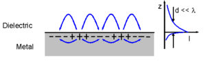
1099:
754:
227:
whereas another maskless approach by Pan et al. uses a "multi-stage plasmonic lens" for progressive coupling.
1181:
1151:
1146:
554:
552:
Chaturvedi1, Pratik; Wu, Wei; Logeeswaran, VJ; et al. (25 January 2010). "A smooth optical superlens".
385:
327:
Xie, Zhihua; Yu, Weixing; Wang, Taisheng; et al. (31 May 2011). "Plasmonic nanolithography: a review".
285:
383:
Shao, D. B.; Chen, S. C. (2005). "Surface-plasmon-assisted nanoscale photolithography by polarized light".
1221:
808:
295:
290:
222:
of incoming light beyond the diffraction limit. Chaturvedi et al. has demonstrated the imaging of a 30 nm
656:
583:
505:
1196:
859:
800:
665:
618:
563:
460:
423:
412:
Srituravanich, Werayut; Fang, Nicholas; Sun, Cheng; et al. (2004). "Plasmonic nanolithography".
256:
231:
78:
813:
1273:
1226:
1186:
966:
142:
114:
1201:
705:
449:
Liu, Zhao-Wei; Wei, Qi-Huo; Zhang, Xiang (2005). "Surface plasmon interference nanolithography".
90:
48:
117:
coupling methods are common. For plasmonic nanolithography processes, this is achieved through
43:
that propagate in between planar dielectric-metal layers in the optical regime, can bypass the
1191:
1078:
983:
946:
877:
826:
771:
734:
681:
636:
534:
499:
Chen, Hao; Bhuiya, Abdul M.; Ding, Qing; Johnson, Harley T.; Toussaint Jr., Kimani C. (2016).
476:
363:
175:
167:
1211:
1136:
1070:
1041:
1012:
975:
938:
909:
867:
818:
763:
724:
714:
673:
626:
571:
524:
514:
468:
431:
394:
336:
264:
192:
98:
52:
28:
1247:
1122:
32:
767:
863:
804:
669:
622:
567:
464:
427:
1242:
850:
729:
700:
609:
529:
500:
260:
243:
219:
204:
110:
1262:
171:
40:
791:
451:
414:
82:
501:"Towards do-it-yourself planar optical components using plasmon-assisted etching"
1074:
215:
150:
149:, on which the SPPs are excited. Similar to common photolithographic processes,
129:
964:
Wang, Shuangshuang; Ding, Tao (2019). "Plasmon-assisted nanojet lithography".
340:
106:
101:
that decay perpendicularly to the interface where the propagation occurs. The
699:
Pan, Liang; Park, Yongshik; Xiong, Yi; Ulin-Avila, Erick (29 November 2011).
211:
163:
146:
134:
1082:
1016:
987:
950:
881:
830:
775:
738:
685:
677:
640:
538:
480:
1166:
195:
via plasmon-assisted etching. In this scheme, etching is achieved through
929:
872:
845:
631:
604:
359:
259:
monolayers in a process termed as "optothermoplasmonic nanolithography."
252:
223:
159:
519:
354:
Maradudin, Alexei A.; Sambles, J. Roy; Barnes, William L., eds. (2014).
145:, a modification on the evanescent near-field lithography, uses a metal
1045:
979:
94:
942:
913:
822:
719:
575:
472:
435:
398:
155:
86:
1091:
180:
846:"Plasmonic nano lithography with a high scan speed contact probe"
1095:
605:"193nm superlens imaging structure for 20nm lithography node"
844:
Kim, Yongwoo; Kim, Seok; Jung, Howon; et al. (2009).
81:
that propagate in between two surfaces with sign-changing
39:(SPPs) to fabricate nanoscale structures. SPPs, which are
247:
thermal excitations in gold nanoparticles to fabricate
67:
Schematic representation of a surface plasmon polariton
701:"Maskless plasmonic lithography at 22 nm resolution"
1235:
1174:
1129:
603:Shi, Zhong; Kochergin, Vladimir; Wang, Fei (2009).
322:
320:
318:
316:
314:
312:
310:
893:
891:
494:
492:
490:
1107:
8:
588:: CS1 maint: numeric names: authors list (
51:that acts as a bottleneck for conventional
1114:
1100:
1092:
234:form of photolithography that is based on
1062:The Journal of Physical Chemistry Letters
901:The Journal of Physical Chemistry Letters
871:
812:
728:
718:
630:
528:
518:
203:Planar lens imaging nanolithography uses
128:
62:
306:
77:Surface plasmon polaritons are surface
581:
162:; such structures can be realized by
7:
85:. They originate from coupling of
14:
269:plasmon-induced charge separation
1165:
1033:Journal of Materials Chemistry C
199:resonances in gold nanoantennas.
214:, which were first proposed by
1269:Lithography (microfabrication)
768:10.1088/0957-4484/19/02/025305
230:Plasmonic direct writing is a
1:
1004:Advanced Functional Materials
103:dispersion relation for SPPs
1075:10.1021/acs.jpclett.6b02393
267:substrates by the means of
1290:
249:two-dimensional structures
236:scanning probe lithography
105:permits the excitation of
70:
37:surface plasmon polaritons
25:plasmonic photolithography
1163:
341:10.1007/s11468-011-9237-0
281:Electron-beam lithography
240:localized surface plasmon
73:Surface plasmon polariton
17:Plasmonic nanolithography
1182:Molecular self-assembly
555:Applied Physics Letters
386:Applied Physics Letters
286:Nanoimprint lithography
1017:10.1002/adfm.201803990
678:10.1038/nnano.2008.303
296:Plasmonic metamaterial
291:Nanosphere lithography
200:
138:
68:
31:process that utilizes
657:Nature Nanotechnology
506:Nature Communications
191:
176:interference patterns
133:A general scheme for
132:
79:electromagnetic waves
66:
21:plasmonic lithography
873:10.1364/OE.17.019476
632:10.1364/OE.17.011309
257:molybdenum disulfide
164:thin film deposition
35:excitations such as
864:2009OExpr..1719476K
858:(22): 19476–19485.
805:2008NanoL...8.3041W
670:2008NatNa...3..733S
623:2009OExpr..1711309S
568:2010ApPhL..96d3102C
520:10.1038/ncomms10468
465:2005NanoL...5..957L
428:2004NanoL...4.1085S
143:contact lithography
91:plasma oscillations
1202:Magnetolithography
1046:10.1039/C7TC00379J
980:10.1039/C8NR08834A
706:Scientific Reports
617:(3): 11309–11314.
251:such as patterned
244:Gold nanoparticles
238:; the method uses
220:Fourier components
201:
139:
121:and perforations.
69:
49:optical resolution
1256:
1255:
1069:(21): 4363–4368.
1040:(23): 5628–5642.
974:(19): 9593–9597.
943:10.1021/nn402124p
914:10.1021/jz9002923
823:10.1021/nl8023824
720:10.1038/srep00175
576:10.1063/1.3293448
473:10.1021/nl0506094
436:10.1021/nl049573q
399:10.1063/1.1951052
356:Modern Plasmonics
189:
119:surface roughness
99:evanescent fields
97:. SPPs result in
45:diffraction limit
1281:
1169:
1116:
1109:
1102:
1093:
1087:
1086:
1056:
1050:
1049:
1027:
1021:
1020:
998:
992:
991:
961:
955:
954:
937:(9): 7648–7653.
924:
918:
917:
895:
886:
885:
875:
841:
835:
834:
816:
799:(9): 3041–3045.
786:
780:
779:
749:
743:
742:
732:
722:
696:
690:
689:
651:
645:
644:
634:
600:
594:
593:
587:
579:
549:
543:
542:
532:
522:
496:
485:
484:
446:
440:
439:
422:(6): 1085–1088.
409:
403:
402:
380:
374:
373:
362:. p. 1–23.
351:
345:
344:
324:
265:titanium dioxide
205:plasmonic lenses
193:Optical trapping
190:
168:Bowtie apertures
53:photolithography
29:nanolithographic
1289:
1288:
1284:
1283:
1282:
1280:
1279:
1278:
1259:
1258:
1257:
1252:
1248:Nanoelectronics
1231:
1170:
1161:
1125:
1123:Nanolithography
1120:
1090:
1058:
1057:
1053:
1029:
1028:
1024:
1011:(41): 1870299.
1000:
999:
995:
963:
962:
958:
926:
925:
921:
897:
896:
889:
843:
842:
838:
814:10.1.1.862.5284
788:
787:
783:
751:
750:
746:
698:
697:
693:
664:(12): 733–737.
653:
652:
648:
602:
601:
597:
580:
551:
550:
546:
498:
497:
488:
448:
447:
443:
411:
410:
406:
382:
381:
377:
370:
353:
352:
348:
326:
325:
308:
304:
277:
181:
127:
93:, quantized as
75:
61:
33:surface plasmon
19:(also known as
12:
11:
5:
1287:
1285:
1277:
1276:
1271:
1261:
1260:
1254:
1253:
1251:
1250:
1245:
1243:Nanotechnology
1239:
1237:
1233:
1232:
1230:
1229:
1224:
1219:
1217:Laser printing
1214:
1209:
1204:
1199:
1194:
1189:
1184:
1178:
1176:
1172:
1171:
1164:
1162:
1160:
1159:
1157:Scanning probe
1154:
1149:
1144:
1139:
1133:
1131:
1127:
1126:
1121:
1119:
1118:
1111:
1104:
1096:
1089:
1088:
1051:
1022:
993:
956:
919:
908:(3): 657–662.
887:
851:Optics Express
836:
781:
755:Nanotechnology
744:
691:
646:
610:Optics Express
595:
544:
486:
459:(5): 957–961.
441:
404:
393:(25): 253107.
375:
368:
346:
335:(3): 565–580.
305:
303:
300:
299:
298:
293:
288:
283:
276:
273:
209:negative-index
126:
123:
83:permittivities
71:Main article:
60:
57:
13:
10:
9:
6:
4:
3:
2:
1286:
1275:
1272:
1270:
1267:
1266:
1264:
1249:
1246:
1244:
1241:
1240:
1238:
1234:
1228:
1225:
1223:
1220:
1218:
1215:
1213:
1210:
1208:
1205:
1203:
1200:
1198:
1195:
1193:
1190:
1188:
1185:
1183:
1180:
1179:
1177:
1173:
1168:
1158:
1155:
1153:
1150:
1148:
1145:
1143:
1142:Electron beam
1140:
1138:
1135:
1134:
1132:
1128:
1124:
1117:
1112:
1110:
1105:
1103:
1098:
1097:
1094:
1084:
1080:
1076:
1072:
1068:
1064:
1063:
1055:
1052:
1047:
1043:
1039:
1035:
1034:
1026:
1023:
1018:
1014:
1010:
1006:
1005:
997:
994:
989:
985:
981:
977:
973:
969:
968:
960:
957:
952:
948:
944:
940:
936:
932:
931:
923:
920:
915:
911:
907:
903:
902:
894:
892:
888:
883:
879:
874:
869:
865:
861:
857:
853:
852:
847:
840:
837:
832:
828:
824:
820:
815:
810:
806:
802:
798:
794:
793:
785:
782:
777:
773:
769:
765:
762:(2): 025305.
761:
757:
756:
748:
745:
740:
736:
731:
726:
721:
716:
712:
708:
707:
702:
695:
692:
687:
683:
679:
675:
671:
667:
663:
659:
658:
650:
647:
642:
638:
633:
628:
624:
620:
616:
612:
611:
606:
599:
596:
591:
585:
577:
573:
569:
565:
562:(4): 043102.
561:
557:
556:
548:
545:
540:
536:
531:
526:
521:
516:
512:
508:
507:
502:
495:
493:
491:
487:
482:
478:
474:
470:
466:
462:
458:
454:
453:
445:
442:
437:
433:
429:
425:
421:
417:
416:
408:
405:
400:
396:
392:
388:
387:
379:
376:
371:
369:9780444595263
365:
361:
358:. Amsterdam:
357:
350:
347:
342:
338:
334:
330:
323:
321:
319:
317:
315:
313:
311:
307:
301:
297:
294:
292:
289:
287:
284:
282:
279:
278:
274:
272:
270:
266:
262:
261:Photochemical
258:
254:
250:
245:
241:
237:
233:
228:
225:
221:
217:
213:
210:
206:
198:
194:
179:
177:
173:
169:
165:
161:
157:
152:
148:
144:
136:
131:
124:
122:
120:
116:
112:
108:
104:
100:
96:
92:
88:
84:
80:
74:
65:
58:
56:
54:
50:
46:
42:
41:surface waves
38:
34:
30:
26:
22:
18:
1206:
1066:
1060:
1054:
1037:
1031:
1025:
1008:
1002:
996:
971:
965:
959:
934:
928:
922:
905:
899:
855:
849:
839:
796:
792:Nano Letters
790:
784:
759:
753:
747:
713:(175): 175.
710:
704:
694:
661:
655:
649:
614:
608:
598:
584:cite journal
559:
553:
547:
513:(7): 10468.
510:
504:
456:
452:Nano Letters
450:
444:
419:
415:Nano Letters
413:
407:
390:
384:
378:
355:
349:
332:
328:
229:
202:
140:
76:
24:
20:
16:
15:
1227:Proton beam
1152:Multiphoton
1147:Nanoimprint
216:John Pendry
212:superlenses
151:photoresist
137:lithography
107:wavelengths
1274:Plasmonics
1263:Categories
1222:Nanosphere
329:Plasmonics
302:References
141:Plasmonic
1207:Plasmonic
967:Nanoscale
809:CiteSeerX
166:methods.
147:photomask
135:photomask
1236:See also
1197:Ion beam
1083:27767323
988:31063168
951:23941522
930:ACS Nano
882:19997168
831:18720976
776:21817542
739:22355690
686:19057593
641:19582044
539:26814026
481:15884902
360:Elsevier
275:See also
253:graphene
232:maskless
224:chromium
172:nanogaps
160:aperture
95:plasmons
1187:Stencil
1137:Optical
860:Bibcode
801:Bibcode
730:3240963
666:Bibcode
619:Bibcode
564:Bibcode
530:4737853
461:Bibcode
424:Bibcode
125:Methods
115:grating
87:photons
47:on the
27:) is a
1081:
986:
949:
880:
829:
811:
774:
737:
727:
684:
639:
537:
527:
479:
366:
156:silver
59:Theory
1192:X-ray
1175:Other
111:prism
1212:Soft
1130:Main
1079:PMID
984:PMID
947:PMID
878:PMID
827:PMID
772:PMID
735:PMID
682:PMID
637:PMID
590:link
535:PMID
477:PMID
364:ISBN
255:and
170:and
113:and
1071:doi
1042:doi
1013:doi
976:doi
939:doi
910:doi
868:doi
819:doi
764:doi
725:PMC
715:doi
674:doi
627:doi
572:doi
525:PMC
515:doi
469:doi
432:doi
395:doi
337:doi
207:or
197:LSP
89:to
23:or
1265::
1077:.
1065:.
1036:.
1009:28
1007:.
982:.
972:11
970:.
945:.
933:.
904:.
890:^
876:.
866:.
856:17
854:.
848:.
825:.
817:.
807:.
795:.
770:.
760:19
758:.
733:.
723:.
709:.
703:.
680:.
672:.
660:.
635:.
625:.
615:17
613:.
607:.
586:}}
582:{{
570:.
560:96
558:.
533:.
523:.
509:.
503:.
489:^
475:.
467:.
455:.
430:.
418:.
391:86
389:.
331:.
309:^
271:.
55:.
1115:e
1108:t
1101:v
1085:.
1073::
1067:7
1048:.
1044::
1038:5
1019:.
1015::
990:.
978::
953:.
941::
935:7
916:.
912::
906:1
884:.
870::
862::
833:.
821::
803::
797:8
778:.
766::
741:.
717::
711:1
688:.
676::
668::
662:3
643:.
629::
621::
592:)
578:.
574::
566::
541:.
517::
511:7
483:.
471::
463::
457:5
438:.
434::
426::
420:4
401:.
397::
372:.
343:.
339::
333:6
Text is available under the Creative Commons Attribution-ShareAlike License. Additional terms may apply.