688:
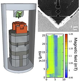
Nitrogen is used. During non-contact, non-destructive imaging of room temperature samples in air, the system achieves a raw, unprocessed spatial resolution equal to the distance separating the sensor from the current or the effective size of the sensor, whichever is larger. To best locate a wire short in a buried layer, however, a Fast
Fourier Transform (FFT) back-evolution technique can be used to transform the magnetic field image into an equivalent map of the current in an integrated circuit or printed wiring board. The resulting current map can then be compared to a circuit diagram to determine the fault location. With this post-processing of a magnetic image and the low noise present in SQUID images, it is possible to enhance the spatial resolution by factors of 5 or more over the near-field limited magnetic image. The system's output is displayed as a false-color image of magnetic field strength or current magnitude (after processing) versus position on the sample. After processing to obtain current magnitude, this microscope has been successful at locating shorts in conductors to within ±16 μm at a sensor-current distance of 150 μm.
1335:
For purposes of this paper the top-down X-ray view shows the x-y plane of the module. The side view shows the x-z plane, and the end view shows the y-z plane. No anomalies were noted in the radiographic images. Excellent alignment of components on the mini-boards permitted an uncluttered top-down view of the mini-circuit boards. The internal construction of the module was seen to consist of eight, stacked mini-boards, each with a single microcircuit and capacitor. The mini-boards connected with the external module pins using the gold-plated exterior of the package. External inspection showed that laser-cut trenches created an external circuit on the device, which is used to enable, read, or write to any of the eight EEPROM devices in the encapsulated vertical stack. Regarding nomenclature, the laser-trenched gold panels on the exterior walls of the package were labeled with the pin numbers. The eight miniboards were labeled TSOP01 through TSOP08, beginning at the bottom of the package near the device pins.
1287:
superconducting sensors. Instruments equipped with such sensors can follow the path of a short circuit along its course through a part. The SQUID detector has been used in failure analysis for many years, and is now commercially available for use at the package level. The ability of SQUID to track the flow of current provides a virtual roadmap of the short, including the location in plan view of the shorting material in a package. We used the SQUID facilities at
Neocera to investigate the failure in the package of interest, with pins carrying 1.47 milliamps at 2 volts. SQUID analysis of the part revealed a clear current path between the two pins of interest, including the location of the conductive material that bridged the two pins. The SQUID scan of the part is shown in Figure 1.
1187:
is only half the task; fault localization is still necessary. The critical step is to overlay the SSM current images or current path images with CAD files such as bonding diagrams or RTX images to pinpoint the fault location. To make alignment of overlaying possible, an optical two-point reference alignment is made. The package edge and package fiducial are the most convenient package markings to align to. Based on the data analysis, fault localization by SSM should isolate the short in the die, bond wires or package substrate. After all non-destructive approaches are exhausted, the final step is destructive deprocessing to verify SSM data. Depending on fault isolation, the deprocessing techniques include decapsulation, parallel lapping or cross-section.
1183:
analysis, and Real-Time X-ray (RTX) inspection were the non-destructive tools used to detect short faults. Unfortunately, these techniques do not work very well in advanced wire-bond packages. Because of the high density wire bonding in advanced wire-bond packages, it is extremely hard to localize the short with conventional RTX inspection. Without detailed information as to where the short might occur, attempting destructive decapsulation to expose both die surface and bond wires is full of risk. Wet chemical etching to remove mold compound in a large area often results in over-etching. Furthermore, even if the package is successfully decapped, visual inspection of the multi-tiered bond wires is a blind search.
1339:
wide trace on the mini-boards. All of the Vss pins were shorted to the Vcc pins with a resistance determined by the I-V slope at approximately 1.74 ohms, the low resistance indicating something other than an ESD defect. Similarly electrical overstress was considered an unlikely cause of failure as the part had not been under power since the time it was qualified at the factory. The three-dimensional geometry of the EEPROM module suggested the use of magnetic current imaging (MCI) on three, or more flat sides in order to construct the current path of the short within the module. As noted, the coordinate axes selected for this analysis are shown in Figure 1.
1239:
of the package. Based on electrical and layout analysis of the package, it can be inferred that current is either flowing through the wirebond pads or that the wirebonds are somehow touching a conductive structure at the specified location. After obtaining similar SSM results on the two units under test, further destructive analysis focused around the small potential short region, and it showed that the failing pin wirebond is touching the bottom of one of the stacked dice at the specific XY position highlighted by SSM analysis. The cross section view of one of those units is shown in figure 3.
1167:
756:. When the SQUID is biased with a constant current that exceeds the critical current of the junction, then changes in the magnetic flux, Φ, threading the SQUID loop produce changes in the voltage drop across the SQUID (see Figure 1). Figure 2(a) shows the I-V characteristic of a SQUID where ∆V is the modulation depth of the SQUID due to external magnetic fields. The voltage across a SQUID is a nonlinear periodic function of the applied magnetic field, with a periodicity of one flux quantum, Φ
1348:
wide), although software and data acquisition improvements allow locating currents within 3 micrometres. To operate, the SQUID sensor must be kept cool (about 77 K) and in vacuum, while the sample, at room temperature, is raster-scanned under the sensor at some working distance z, separated from the SQUID enclosure by a thin, transparent diamond window. This allows one to reduce the scanning distance to tens of micrometres from the sensor itself, improving the resolution of the tool.
504:. To use the DC SQUID to measure standard magnetic fields, one must either count the number of oscillations in the voltage as the field is changed, which is very difficult in practice, or use a separate DC bias magnetic field parallel to the device to maintain a constant voltage and consequently constant magnetic flux through the loop. The strength of the field being measured will then be equal to the strength of the bias magnetic field passing through the SQUID.
1223:
1215:
1207:
1296:
point that radiography can now be used to identify features heretofore impossible to detect. The equipment at Xradia was used to inspect the failure of interest in this analysis. An example of their findings is shown in Figure 2. The feature shown (which is also the material responsible for the failure) is a copper filament approximately three micrometres wide in cross-section, which was impossible to resolve in our in-house radiography equipment.
760:=2.07×10 Tm (see Figure 2(b)). In order to convert this nonlinear response to a linear response, a negative feedback circuit is used to apply a feedback flux to the SQUID so as to keep the total flux through the SQUID constant. In such a flux locked loop, the magnitude of this feedback flux is proportional to the external magnetic field applied to the SQUID. Further description of the physics of SQUIDs and SQUID microscopy can be found elsewhere.
1231:
defect locations; however, defects like metal migration produced at wirebond pads, or bond wires somehow touching any other conductive structures, may be very difficult to catch with non-destructive techniques that are not electrical in nature. Here, the availability of analytical tools that can map out the flow of electric current inside the package provide valuable information to guide the failure analyst to potential defect locations.
31:
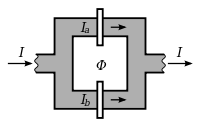
752:, cooled below 80K and in vacuum while the device under test is at room temperature and in air. A SQUID consists of two Josephson tunnel junctions that are connected together in a superconducting loop (see Figure 1). A Josephson junction is formed by two superconducting regions that are separated by a thin insulating barrier. Current exists in the junction without any voltage drop, up to a maximum value, called the critical current, I
1270:
1262:
1278:
with conventional radiographic analysis were unsuccessful. Arguably the most difficult part of the procedure is identifying the physical location of the short with a high enough degree of confidence to permit destructive techniques to be used to reveal the shorting material. Fortunately, two analytical techniques are now available that can significantly increase the effectiveness of the fault localization process.
1300:
both time and money to perform. In effect, to get the most out of it, the analyst really needs to know already where the failure is located. This makes low-power radiography a useful supplement to SQUID, but not a generally effective replacement for it. It would likely best be used immediately after SQUID to characterize morphology and depth of the shorting material once SQUID had pinpointed its location.
668:
2148:
902:
437:
697:
115:
713:
1175:
1326:
1318:
1309:
1235:
inconsistently failing and recovering under reliability tests. Time domain reflectometry and X-ray analysis were performed on these units with no success in isolating the defects. Also there was no clear indication of defects that could potentially produce the observed electrical short failure mode. Two of those units were analyzed with SSM.
1352:
another, getting closer to the sensor in the process, this will be revealed as stronger magnetic field intensity for the section closer to the sensor and also as higher intensity in the current density map. This way, vertical information can be extracted from the current density images. Further details about MCI can be found elsewhere.
655:. Depending on the particular application, different levels of precision may be required in the height of the apparatus. Operating at lower-tip sample distances increases the sensitivity and resolution of the device, but requires more advanced mechanisms in controlling the height of the probe. In addition such devices require extensive
1351:
The typical MCI sensor configuration is sensitive to magnetic fields in the perpendicular z direction (i.e., sensitive to the in-plane xy current distribution in the DUT). This does not mean that we are missing vertical information; in the simplest situation, if a current path jumps from one plane to
1338:
Pin-to-pin electrical testing confirmed that Vcc Pins 12, 13, 14, and 15 were electrically common, presumably through the common exterior gold panel on the package wall. Likewise, Vss Pins 24, 25, 26, and 27 were common. Comparison to the xray images showed that these four pins funneled into a single
1069:
of a single YBCO crystal (figure). In a
Josephson junction ring the superconducting electrons form a coherent wave function, just as in a superconductor. As the wavefunction must have only one value at each point, the overall phase factor obtained after traversing the entire Josephson circuit must be
1555:
L. A. Knauss, B. M. Frazier, H. M. Christen, S. D. Silliman and K. S. Harshavardhan, Neocera LLC, 10000 Virginia Manor Rd. Beltsville, MD 20705, E. F. Fleet and F. C. Wellstood, Center for
Superconductivity Research, University of Maryland at College Park College Park, MD 20742, M. Mahanpour and A.
1238:
Electrically connecting the failing pin to a ground pin produced the electric current path shown in figure 2. This electrical path strongly suggests that the current is somehow flowing through all the ground nets though a conductive path located very close to the wirebond pads from the top down view
892:
As a result, the current can be directly calculated from the magnetic field knowing only the separation between the current and the magnetic field sensor. The details of this mathematical calculation can be found elsewhere, but what is important to know here is that this is a direct calculation that
687:
of current at a distance of 100 μm from the SQUID sensor with 1 second averaging. The microscope uses a patented design to allow the sample under investigation to be at room temperature and in air while the SQUID sensor is under vacuum and cooled to less than 80 K using a cryo cooler. No Liquid
1334:
Examination of the module shown in Figure 1 in the
Failure Analysis Laboratory found no external evidence of the failure. Coordinate axes of the device were chosen as shown in Figure 1. Radiography was performed on the module in three orthogonal views: side, end, and top-down; as shown in Figure 2.
1299:
The principal drawback of this technique is that the depth of field is extremely short, requiring many ‘cuts’ on a given specimen to detect very small particles or filaments. At the high magnification required to resolve micrometre-sized features, the technique can become prohibitively expensive in
1277:
The failure in this example was characterized as an eight-ohm short between two adjacent pins. The bond wires to the pins of interest were cut with no effect on the short as measured at the external pins, indicating that the short was present in the package. Initial attempts to identify the failure
1186:
The
Scanning SQUID Microscopy (SSM) data are current density images and current peak images. The current density images give the magnitude of the current, while the current peak images reveal the current path with a ± 3 μm resolution. Obtaining the SSM data from scanning advanced wire-bond packages
1182:
Advanced wire-bond packages, unlike traditional Ball Grid Array (BGA) packages, have multiple pad rows on the die and multiple tiers on the substrate. This package technology has brought new challenges to failure analysis. To date, Scanning
Acoustic Microscopy (SAM), Time Domain Reflectometry (TDR)
630:
should be chosen. The SQUID itself can be used as the pickup coil for measuring the magnetic field, in which case the resolution of the device is proportional to the size of the SQUID. However, currents in or near the SQUID generate magnetic fields which are then registered in the coil and can be a
735:
the tip across the area where measurements are desired. As the change in voltage corresponding to the measured magnetic field is quite rapid, the strength of the bias magnetic field is typically controlled by feedback electronics. This field strength is then recorded by a computer system that also
1295:
The second fault location technique will be taken somewhat out of turn, as it was used to characterize this failure after the SQUID analysis, as an evaluation sample for an equipment vendor. The ability to focus and resolve low-power X-rays and detect their presence or absence has improved to the
1230:
Electric shorts in multi-stacked die packages can be very difficult to isolate non-destructively; especially when a large number of bond wires are somehow shorted. For instance, when an electric short is produced by two bond wires touching each other, X-ray analysis may help to identify potential
639:
of the device, and limitations in the control of the bias magnetic field as well as electronics issues prevent a perfectly constant voltage from being maintained at all times. However, in practice, the sensitivity in most scanning SQUID microscopes is sufficient for almost any SQUID size for many
1347:
SQUIDs are the most sensitive magnetic sensors known. This allows one to scan currents of 500 nA at a working distance of about 400 micrometres. As for all near field situations, the resolution is limited by the scanning distance or, ultimately, by the sensor size (typical SQUIDs are about 30 μm
1234:
Figure 1a shows the schematic of our first case study consisting of a triple-stacked die package. The X-ray image of figure 1b is intended to illustrate the challenge of finding the potential short locations represented for failure analysts. In particular, this is one of a set of units that were
1286:
One characteristic that all shorts have in common is the movement of electrons from a high potential to a lower one. This physical movement of the electrical charge creates a small magnetic field around the electron. With enough electrons moving, the aggregate magnetic field can be detected by
739:
As the name implies, SQUIDs are made from superconducting material. As a result, they need to be cooled to cryogenic temperatures of less than 90 K (liquid nitrogen temperatures) for high temperature SQUIDs and less than 9 K (liquid helium temperatures) for low temperature SQUIDs. For magnetic
631:
source of noise. To reduce this effect it is also possible to make the size of the SQUID itself very small, but attach the device to a larger external superconducting loop located far from the SQUID. The flux through the loop will then be detected and measured, inducing a voltage in the SQUID.
1993:
Wills, K.S., Diaz de Leon, O., Ramanujachar, K., and Todd, C., “Super-conducting
Quantum Interference Device Technique: 3-D Localization of a Short within a Flip Chip Assembly,” Proceedings of the 27th International Symposium for Testing and Failure Analysis, San Jose, CA, November, 2001, pp.
515:, is also emitted in the bias coil. This AC field produces an AC voltage with amplitude proportional to the DC component in the SQUID. The advantage of this technique is that the frequency of the voltage signal can be chosen to be far away from that of any potential noise sources. By using a
238:
2003:"Construction of a 3-D Current Path Using Magnetic Current Imaging", ISTFA 2007, Frederick Felt, NASA Goddard Space Flight Center, Greenbelt, MD, USA, Lee Knauss, Neocera, Beltsville, MD, USA, Anders Gilbertson, Neocera, Beltsville, MD, USA, Antonio Orozco, Neocera, Beltsville, MD, USA
1984:"A Procedure for Identifying the Failure Mechanism Responsible for A Pin-To-Pin Short Within Plastic Mold Compound Integrated Circuit Packages", ISTFA 2008, Carl Nail, Jesus Rocha, and Lawrence Wong National Semiconductor Corporation, Santa Clara, California, United States
1089:)π will be observed. Compared to the case of standard s-wave junctions, where no phase shift is observed, no anomalous effects were expected in the B, C, and D cases, as the single valued property is conserved, but for device A, the system must do something to for the φ=2
768:
Magnetic current imaging uses the magnetic fields produced by currents in electronic devices to obtain images of those currents. This is accomplished through the fundamental physics relationship between magnetic fields and current, the Biot-Savart Law:
880:
893:
is not influenced by other materials or effects, and that through the use of Fast
Fourier Transforms these calculations can be performed very quickly. A magnetic field image can be converted to a current density image in about 1 or 2 seconds.
499:
with respect to the amount of magnetic flux passing through the device. As a result, alone a SQUID can only be used to measure the change in magnetic field from some known value, unless the magnetic field or device size is very small such that
1329:
Figure 3: A magnetic current image overlay on an X-ray image of the EEPROM module. Thresholding was used to show only the strongest current at the capacitor of the TSOP08 mini-board. Arrows indicate Vcc and Vss pins. This image is in the x-y
1093:π condition to be maintained. In the same property behind the scanning SQUID microscope, the phase of the wavefunction is also altered by the amount of magnetic flux passing through the junction, following the relationship Δφ=π(Φ
432:{\displaystyle {\begin{aligned}V&={\frac {R}{2}}{\sqrt {I^{2}-I_{0}^{2}}},\\&={\frac {R}{2}}\left(I^{2}-\left(2I_{c}\cos \left(\pi {\frac {\Phi }{\Phi _{0}}}\right)\right)^{2}\right)^{\frac {1}{2}},\end{aligned}}}
634:
The resolution and sensitivity of the device are both proportional to the size of the SQUID. A smaller device will have greater resolution but less sensitivity. The change in voltage induced is proportional to the
1040:
1312:
Figure 1: An external view of the EEPROM module shows the coordinate axis used while performing orthogonal magnetic current imaging. These axes are used to define the scanning planes in the body of the
543:
can map out buried current-carrying wires by measuring the magnetic fields produced by the currents, or can be used to image fields produced by magnetic materials. By mapping out the current in an
1800:
Tsuei, C.C.; J. R. Kirtley; C. C. Chi; Lock See Yu-Jahnes; A. Gupta; T. Shaw; J. Z. Sun; M. B. Ketchen (1994). "Pairing
Symmetry and Flux Quantization in a Tricrystal Superconducting Ring of YBa
243:
1537:
J. P. Wikswo, Jr. “The Magnetic Inverse Problem for NDE”, in H. Weinstock (ed.), SQUID Sensors: Fundamentals, Fabrication, and Applications, Kluwer Academic Publishers, pp. 629-695, (1996)
1073:
In YBCO, upon crossing the planes in momentum (and real) space, the wavefunction will undergo a phase shift of π. Hence if one forms a Josephson ring device where this plane is crossed (2
1123:
Scanning SQUID Microscope can detect all types of shorts and conductive paths including Resistive Opens (RO) defects such as cracked or voided bumps, Delaminated Vias, Cracked traces/
1120:
was the area of the ring. The device observed zero field at B, C, and D. The results provided one of the earliest and most direct experimental confirmations of d-wave pairing in YBCO.
912:
The scanning SQUID microscope was originally developed for an experiment to test the pairing symmetry of the high-temperature cuprate superconductor YBCO. Standard superconductors are
1042:, meaning that when crossing over any of the directions in momentum space one will observe a sign change in the order parameter. The form of this function is equal to that of the
86:, the scanning SQUID microscope allows magnetic fields to be measured with unparalleled resolution and sensitivity. The first scanning SQUID microscope was built in 1992 by Black
1463:
Black, R.C.; A. Mathai; and F. C. Wellstood; E. Dantsker; A. H. Miklich; D. T. Nemeth; J. J. Kingston; J. Clarke (1993). "Magnetic microscopy using a liquid nitrogen cooled YBa
2339:
2075:
577:
squid and maintaining thermal separation with the sample. In either case, due to the extreme sensitivity of the SQUID probe to stray magnetic fields, in general some form of
1108:
used a scanning SQUID microscope to measure the local magnetic field at each of the devices in the figure, and observed a field in ring A approximately equal in magnitude Φ
775:
1975:"Scanning SQUID Microscopy for New Package Technologies", ISTFA 2004, Mario Pacheco and Zhiyong Wang Intel Corporation, 5000 W. Chandler Blvd., Chandler, AZ, U.S.A., 85226
82:
near the surface of the sample to be measured. As the SQUID is the most sensitive detector of magnetic fields available and can be constructed at submicrometre widths via
740:
current imaging systems, a small (about 30 μm wide) high temperature SQUID is used. This system has been designed to keep a high temperature SQUID, made from YBa
644:
techniques it is possible to fabricate devices with total area of 1–10 μm, although devices in the tens to hundreds of square micrometres are more common.
210:
190:
163:
2130:
1070:
an integer multiple of 2π, as otherwise, one would obtain a different value of the probability density depending on the number of times one traversed the ring.
934:
136:
511:
technique is used. In addition to the DC bias magnetic field, an AC magnetic field of constant amplitude, with field strength generating Φ << Φ
1050:
function, giving it the name d-wave superconductivity. As the superconducting electrons are described by a single coherent wavefunction, proportional to exp(-
2135:
1934:
507:
Although it is possible to read the DC voltage between the two terminals of the SQUID directly, because noise tends to be a problem in DC measurements, an
63:
1890:
Sood, Bhanu; Pecht, Michael (2011-08-11). "Conductive filament formation in printed circuit boards: effects of reflow conditions and flame retardants".
1575:
Fleet, E.F.; Chatraphorn, S.; Wellstood, F.C.; Green, S.M.; Knauss, L.A. (1999). "HTS scanning SQUID microscope cooled by a closed-cycle refrigerator".
1210:
Figure 1(a) Schematic showing typical bond wires in a triple-stacked die package, Figure 1(b) X-ray lateral view of actual triple-stacked die package.
651:
and operated either in direct contact with or just above the sample surface. The position of the SQUID is usually controlled by some form of electric
2012:
L. A. Knauss et al., "Current Imaging using Magnetic Field Sensors". Microelectronics Failure Analysis Desk Reference 5th Ed., pages 303-311 (2004).
1097:). As was predicted by Sigrist and Rice, the phase condition can then be maintained in the junction by a spontaneous flux in the junction of value Φ
2118:
2068:
1678:
Chatraphorn, S.; Fleet, E. F.; Wellstood, F. C.; Knauss, L. A.; Eiles, T. M. (17 April 2000). "Scanning SQUID microscopy of integrated circuits".
1273:
Figure 2: High-resolution radiographic image of filament, measured at 2.9 micrometres wide. Image shows filament running under both shorted leads.
550:
As the SQUID material must be superconducting, measurements must be performed at low temperatures. Typically, experiments are carried out below
2195:
2165:
736:
keeps track of the position of the probe. An optical camera can also be used to track the position of the SQUID with respect to the sample.
2247:
2242:
2227:
2190:
2113:
2375:
2103:
2061:
1519:
947:
95:
724:
respectively. Figure 2 b) Periodic voltage response due to flux through a SQUID. The periodicity is equal to one flux quantum, Φ
2257:
2222:
547:
or a package, short circuits can be localized and chip designs can be verified to see that current is flowing where expected.
2365:
2237:
2217:
2212:
2175:
1855:
Sigrist, Manfred; T. M. Rice (1992). "Paramagnetic Effect in High T c Superconductors -A Hint for d-Wave Superconductivity".
1218:
Figure 2: Overlay of current density, optical, and CAD images in triple-stacked die package with electric short failure mode.
944:
will be the same. However, in the high-temperature cuprate superconductors, the order parameter instead follows the equation
2180:
2125:
91:
1406:
Shibata, Yusuke; Nomura, Shintaro; Kashiwaya, Hiromi; Kashiwaya, Satoshi; Ishiguro, Ryosuke; Takayanagi, Hideaki (2015).
675:
A high temperature Scanning SQUID Microscope using a YBCO SQUID is capable of measuring magnetic fields as small as 20
2277:
2272:
1174:
1166:
2380:
2293:
2207:
2147:
708:
is the critical current of the SQUID, Φ is the flux threading the SQUID and V is the voltage response to that flux.
192:. The thin barriers on each path are Josephson junctions, which together separate the two superconducting regions.
519:
the device can read only the frequency corresponding to the magnetic field, ignoring many other sources of noise.
2360:
2303:
2262:
2185:
2170:
2084:
2034:
680:
1959:
1546:
E.F. Fleet et al., “HTS Scanning SQUID Microscopy of Active Circuits”, Appl. Superconductivity Conference (1998)
2232:
1321:
Figure 2: Radiography, showing three orthogonal views of the part, reveals internal construction of the module.
55:
640:
applications, and therefore the tendency is to make the SQUID as small as possible to enhance resolution. Via
1514:. Vol. I: Fundamentals and Technology of SQUIDs and SQUID Systems. Weinheim: Wiley-VCH. pp. 46–48.
1058:
of the wavefunction, this property can be also interpreted as a phase shift of π under a 90 degree rotation.
2298:
2098:
1936:
Failure Analysis of Short Faults on Advanced Wire-bond and Flip-chip Packages with Scanning SQUID Microscopy
570:
cooling to instead be used. It is even possible to measure room-temperature samples by only cooling a high
585:, possibly in combination with a superconducting "can" (all superconductors repel magnetic fields via the
1132:
2252:
1635:
Wellstood, F.C.; Gim, Y.; Amar, A.; Black, R.C.; Mathai, A. (1997). "Magnetic microscopy using SQUIDs".
1144:
627:
559:
485:
447:
555:
1226:
Figure 3: Cross sectional image showing a bond wire touching the die causing signal to ground leakage.
875:{\displaystyle d{\vec {B}}={\frac {\mu _{0}}{4\pi }}{\frac {Id{\vec {l}}\times {\vec {r}}}{r^{3}}}\,.}
563:
220:
SQUID. A DC SQUID consists of superconducting electrodes in a ring pattern connected by two weak-link
1864:
1821:
1756:
1721:
Wells, Frederick S.; Pan, Alexey V.; Wang, X. Renshaw; Fedoseev, Sergey A.; Hilgenkamp, Hans (2015).
1687:
1644:
1584:
1484:
1419:
593:
1178:
Optical image of the decapped wire bonds that are lifted from the die and touching another wire bond
1143:(MCM) and stacked die. SQUID scanning can also isolate defective components in assembled devices or
1127:
and Cracked Plated Through Holes (PTH). It can map power distributions in packages as well as in 3D
626:
superconductors. In either case, a superconductor with critical temperature higher than that of the
2370:
731:
Operation of a scanning SQUID microscope consists of simply cooling down the probe and sample, and
508:
221:
47:
2043:
916:
with respect to their superconducting properties, that is, for any direction of electron momentum
1951:
1915:
1746:
1608:
1128:
1047:
683:). The SQUID sensor is sensitive enough that it can detect a wire even if it is carrying only 10
641:
578:
544:
1124:
1222:
1214:
1206:
1907:
1837:
1782:
1703:
1660:
1600:
1515:
1445:
1140:
1136:
516:
1408:"Imaging of current density distributions with a Nb weak-link scanning nano-SQUID microscope"
2308:
1943:
1899:
1872:
1829:
1772:
1764:
1695:
1652:
1592:
1492:
1435:
1427:
1381:
1361:
888:
is the permeability of free space, and r is the distance between the current and the sensor.
716:
Figure 2 a) Plot of current vs. voltage for a SQUID. Upper and lower curves correspond to nΦ
455:
75:
195:
168:
141:
30:
2038:
1269:
1261:
937:
605:
586:
567:
225:
1510:
Boris Chesca; Reinhold Kleiner; Dieter Koelle (2004). J. Clarke; A. I. Braginski (eds.).
17:
1868:
1825:
1760:
1691:
1648:
1588:
1488:
1423:
2324:
1777:
1722:
1440:
1407:
919:
905:
652:
600:. A wide variety of superconducting materials can be used, but the two most common are
532:
217:
121:
67:
2354:
1919:
1386:
1055:
732:
551:
477:
79:
43:
1612:
1565:"Current Imaging using Magnetic Field Sensors" L.A. Knauss, S.I. Woods and A. Orozco
1955:
1947:
676:
466:
619: > 77 K and relative ease of deposition compared to other high
1066:
597:
495:. However, as noted by the figure, the voltage across the electrodes oscillates
83:
39:
1833:
1170:
Current Image overlaid the optical image of the part and the layout of the part
667:
2334:
2329:
1903:
1371:
1366:
941:
648:
636:
540:
492:
71:
1911:
1723:"Analysis of low-field isotropic vortex glass containing vortex groups in YBa
1707:
1664:
1604:
884:
B is the magnetic induction, Idℓ is an element of the current, the constant μ
2200:
2053:
913:
656:
1933:
Steve K. Hsiung; Kevan V. Tan; Andrew J. Komrowski; Daniel J. D. Sullivan.
1841:
1786:
1449:
901:
1643:(2). Institute of Electrical and Electronics Engineers (IEEE): 3134–3138.
1583:(2). Institute of Electrical and Electronics Engineers (IEEE): 3704–3707.
1085:, or even number of crossings, as in B, C, and D, a phase difference of (2
1065:
by manufacturing a series of YBCO ring Josephson junctions which crossed
1876:
582:
35:
2031:
1556:
Ghaemmaghami, Advanced Micro Devices, One AMD Place Sunnyvale, CA 94088
601:
229:
38:
refrigerator. Green holder for the SQUID probe is attached to a quartz
1768:
1656:
1596:
1431:
1325:
1317:
1308:
212:
represents the magnetic flux entering the inside of the DC SQUID loop.
2108:
1699:
1496:
684:
531:
is a sensitive near-field imaging system for the measurement of weak
2025:
712:
696:
114:
1751:
476:
is the critical current of the Josephson junctions, Φ is the total
50:
of a SQUID probe and a test image of Nb/Au strips recorded with it.
1376:
1324:
1316:
1307:
1268:
1260:
1221:
1213:
1205:
1173:
1165:
900:
711:
695:
666:
536:
103:
29:
609:
496:
99:
2057:
1151:
Short Localization in Advanced Wirebond Semiconductor Package
2044:
Center for Superconductivity Research, University of Maryland
1282:
Superconducting Quantum Interference Device (SQUID) Detection
1265:
Figure 1 SQUID image of package indicating location of short.
2146:
1035:{\displaystyle \Delta (k)=\Delta _{0}(cos(k_{x}a)-(k_{y}a))}
2048:
216:
The scanning SQUID microscope is based upon the thin-film
659:
dampening if precise height control is to be maintained.
535:
by moving a Superconducting Quantum Interference Device (
138:
enters and splits into the two paths, each with currents
228:
of the Josephson junctions, the idealized difference in
604:, due to its relatively good resistance to damage from
562:. However, advances in high-temperature superconductor
27:
Method of imaging magnetic fields at microscopic scales
2032:
Design and applications of a scanning SQUID microscope
1892:
Journal of Materials Science: Materials in Electronics
1081:+1)π will be observed between the two junctions. For 2
950:
922:
778:
241:
198:
171:
144:
124:
34:
Left: Schematic of a scanning SQUID microscope in a
2317:
2286:
2158:
2091:
2028:, one of the pioneers in scanning SQUID microscopy.
1735:
thin films visualized by scanning SQUID microscopy"
491:Hence, a DC SQUID can be used as a flux-to-voltage
78:. A tiny SQUID is mounted onto a tip which is then
1034:
928:
874:
431:
204:
184:
157:
130:
90:Since then the technique has been used to confirm
700:Figure 1: Electrical schematic of a SQUID where I
1246:Short between pins in molding compound package
1242:A similar defect was found in the second unit.
908:in YBCO imaged by the scanning SQUID microscopy
1637:IEEE Transactions on Applied Superconductivity
1577:IEEE Transactions on Applied Superconductivity
1475:superconducting quantum interference device".
1077:+1), number of times, a phase difference of (2
2069:
592:The actual SQUID probe is generally made via
8:
1625:J. Kirtley, IEEE Spectrum p. 40, Dec. (1996)
936:in the superconductor, the magnitude of the
64:superconducting quantum interference device
2076:
2062:
2054:
663:High temperature scanning SQUID microscope
1776:
1750:
1439:
1017:
995:
970:
949:
921:
868:
860:
844:
843:
829:
828:
819:
803:
797:
783:
782:
777:
581:is used. Most common is a shield made of
411:
400:
382:
373:
353:
331:
311:
290:
285:
272:
266:
256:
242:
240:
197:
176:
170:
149:
143:
123:
113:
1533:
1531:
1398:
679:(about 2 million times weaker than the
2151:Typical atomic force microscopy set-up
1061:This property was exploited by Tsuei
940:and consequently the superconducting
7:
764:Magnetic field detection using SQUID
566:have allowed relatively inexpensive
647:The SQUID itself is mounted onto a
232:between the electrodes is given by
118:Diagram of a DC SQUID. The current
967:
951:
379:
375:
199:
25:
1686:(16). AIP Publishing: 2304–2306.
596:with the SQUID area outlined via
66:(SQUID) is used to image surface
1191:Short in multi-stacked packages
96:high-temperature superconductors
92:unconventional superconductivity
2258:Scanning quantum dot microscopy
2213:Photothermal microspectroscopy
1948:10.31399/asm.cp.istfa2004p0073
1029:
1026:
1010:
1004:
988:
976:
960:
954:
849:
834:
788:
554:temperature (4.2 K) in a
1:
1054:φ), where φ is known as the
2196:Near-field scanning optical
2166:Ballistic electron emission
2397:
2294:Scanning probe lithography
1834:10.1103/PhysRevLett.73.593
2376:Scanning probe microscopy
2304:Feature-oriented scanning
2268:Scanning SQUID microscopy
2263:Scanning SQUID microscope
2144:
2085:Scanning probe microscopy
1904:10.1007/s10854-011-0449-z
671:Scanning SQUID microscope
529:Scanning SQUID Microscope
60:scanning SQUID microscopy
18:Scanning SQUID microscope
2248:Scanning joule expansion
2243:Scanning ion-conductance
2228:Scanning electrochemical
2191:Magnetic resonance force
1343:Magnetic Current Imaging
450:between the electrodes,
224:(see figure). Above the
56:condensed matter physics
2299:Dip-pen nanolithography
1680:Applied Physics Letters
1372:Low-Temperature Physics
480:through the ring, and Φ
62:is a technique where a
2152:
1331:
1322:
1314:
1274:
1266:
1227:
1219:
1211:
1179:
1171:
1036:
930:
909:
876:
728:
709:
704:is the bias current, I
681:Earth's magnetic field
672:
539:) across an area. The
433:
213:
206:
186:
159:
132:
51:
2366:Measuring instruments
2253:Scanning Kelvin probe
2150:
1328:
1320:
1311:
1304:Short in a 3D Package
1291:Low-power radiography
1272:
1264:
1225:
1217:
1209:
1177:
1169:
1145:Printed Circuit Board
1037:
931:
904:
877:
715:
699:
670:
628:operating temperature
560:dilution refrigerator
556:helium-3 refrigerator
486:magnetic flux quantum
434:
207:
205:{\displaystyle \Phi }
187:
185:{\displaystyle I_{b}}
160:
158:{\displaystyle I_{a}}
133:
117:
46:sample stage. Right:
33:
2340:Vibrational analysis
2223:Scanning capacitance
1877:10.1143/JPSJ.61.4283
948:
920:
776:
594:thin-film deposition
239:
196:
169:
142:
122:
110:Operating principles
2238:Scanning Hall probe
2218:Piezoresponse force
2176:Electrostatic force
1869:1992JPSJ...61.4283S
1826:1994PhRvL..73..593T
1761:2015NatSR...5E8677W
1692:2000ApPhL..76.2304C
1649:1997ITAS....7.3134W
1589:1999ITAS....9.3704F
1489:1993ApPhL..62.2128B
1424:2015NatSR...515097S
1133:Through-Silicon Via
1129:Integrated Circuits
509:alternating current
295:
222:Josephson junctions
48:electron micrograph
42:. Bottom part is a
2181:Kelvin probe force
2153:
2126:Scanning tunneling
2037:2008-07-06 at the
1739:Scientific Reports
1512:The SQUID Handbook
1412:Scientific Reports
1332:
1323:
1315:
1275:
1267:
1228:
1220:
1212:
1180:
1172:
1048:spherical harmonic
1032:
926:
910:
872:
729:
710:
673:
642:e-beam lithography
579:magnetic shielding
545:integrated circuit
500:Φ < Φ
429:
427:
281:
214:
202:
182:
155:
128:
52:
2381:Superconductivity
2348:
2347:
1898:(10): 1602–1615.
1857:J. Phys. Soc. Jpn
1769:10.1038/srep08677
1657:10.1109/77.621996
1597:10.1109/77.783833
1483:(17): 2128–2130.
1432:10.1038/srep15097
1141:Multi-Chip Module
1137:System in package
929:{\displaystyle k}
866:
852:
837:
817:
791:
517:lock-in amplifier
419:
388:
319:
296:
264:
131:{\displaystyle I}
16:(Redirected from
2388:
2361:Josephson effect
2309:Millipede memory
2278:Scanning voltage
2273:Scanning thermal
2078:
2071:
2064:
2055:
2013:
2010:
2004:
2001:
1995:
1991:
1985:
1982:
1976:
1973:
1967:
1966:
1964:
1958:. Archived from
1941:
1930:
1924:
1923:
1887:
1881:
1880:
1852:
1846:
1845:
1797:
1791:
1790:
1780:
1754:
1718:
1712:
1711:
1700:10.1063/1.126327
1675:
1669:
1668:
1632:
1626:
1623:
1617:
1616:
1572:
1566:
1563:
1557:
1553:
1547:
1544:
1538:
1535:
1526:
1525:
1507:
1501:
1500:
1497:10.1063/1.109448
1477:Appl. Phys. Lett
1460:
1454:
1453:
1443:
1403:
1382:Failure analysis
1362:Josephson Effect
1258:
1257:
1253:
1203:
1202:
1198:
1163:
1162:
1158:
1041:
1039:
1038:
1033:
1022:
1021:
1000:
999:
975:
974:
935:
933:
932:
927:
906:Quantum vortices
881:
879:
878:
873:
867:
865:
864:
855:
854:
853:
845:
839:
838:
830:
820:
818:
816:
808:
807:
798:
793:
792:
784:
564:thin-film growth
438:
436:
435:
430:
428:
421:
420:
412:
410:
406:
405:
404:
399:
395:
394:
390:
389:
387:
386:
374:
358:
357:
336:
335:
320:
312:
304:
297:
294:
289:
277:
276:
267:
265:
257:
226:critical current
211:
209:
208:
203:
191:
189:
188:
183:
181:
180:
164:
162:
161:
156:
154:
153:
137:
135:
134:
129:
21:
2396:
2395:
2391:
2390:
2389:
2387:
2386:
2385:
2351:
2350:
2349:
2344:
2313:
2282:
2208:Photon scanning
2154:
2142:
2131:Electrochemical
2119:Photoconductive
2087:
2082:
2039:Wayback Machine
2022:
2017:
2016:
2011:
2007:
2002:
1998:
1992:
1988:
1983:
1979:
1974:
1970:
1962:
1939:
1932:
1931:
1927:
1889:
1888:
1884:
1854:
1853:
1849:
1814:Phys. Rev. Lett
1811:
1807:
1803:
1799:
1798:
1794:
1734:
1730:
1726:
1720:
1719:
1715:
1677:
1676:
1672:
1634:
1633:
1629:
1624:
1620:
1574:
1573:
1569:
1564:
1560:
1554:
1550:
1545:
1541:
1536:
1529:
1522:
1509:
1508:
1504:
1474:
1470:
1466:
1462:
1461:
1457:
1405:
1404:
1400:
1395:
1358:
1345:
1306:
1293:
1284:
1259:
1255:
1251:
1249:
1248:
1204:
1200:
1196:
1194:
1193:
1164:
1160:
1156:
1154:
1153:
1111:
1100:
1096:
1046: = 2
1013:
991:
966:
946:
945:
938:order parameter
918:
917:
899:
887:
856:
821:
809:
799:
774:
773:
766:
759:
755:
751:
747:
743:
727:
723:
719:
707:
703:
694:
665:
624:
617:
612:, for its high
606:thermal cycling
587:Meissner effect
575:
568:liquid nitrogen
533:magnetic fields
525:
523:Instrumentation
514:
503:
483:
474:
465:is the maximum
464:
426:
425:
378:
369:
365:
349:
345:
341:
340:
327:
326:
322:
321:
302:
301:
268:
249:
237:
236:
194:
193:
172:
167:
166:
145:
140:
139:
120:
119:
112:
28:
23:
22:
15:
12:
11:
5:
2394:
2392:
2384:
2383:
2378:
2373:
2368:
2363:
2353:
2352:
2346:
2345:
2343:
2342:
2337:
2332:
2327:
2325:Nanotechnology
2321:
2319:
2315:
2314:
2312:
2311:
2306:
2301:
2296:
2290:
2288:
2284:
2283:
2281:
2280:
2275:
2270:
2265:
2260:
2255:
2250:
2245:
2240:
2235:
2230:
2225:
2220:
2215:
2210:
2205:
2204:
2203:
2193:
2188:
2186:Magnetic force
2183:
2178:
2173:
2171:Chemical force
2168:
2162:
2160:
2156:
2155:
2145:
2143:
2141:
2140:
2139:
2138:
2136:Spin polarized
2133:
2123:
2122:
2121:
2116:
2111:
2106:
2095:
2093:
2089:
2088:
2083:
2081:
2080:
2073:
2066:
2058:
2052:
2051:
2046:
2041:
2029:
2021:
2020:External links
2018:
2015:
2014:
2005:
1996:
1986:
1977:
1968:
1965:on 2019-02-20.
1925:
1882:
1847:
1820:(4): 593–596.
1809:
1805:
1801:
1792:
1732:
1728:
1724:
1713:
1670:
1627:
1618:
1567:
1558:
1548:
1539:
1527:
1520:
1502:
1472:
1468:
1464:
1455:
1397:
1396:
1394:
1391:
1390:
1389:
1384:
1379:
1374:
1369:
1364:
1357:
1354:
1344:
1341:
1305:
1302:
1292:
1289:
1283:
1280:
1247:
1244:
1192:
1189:
1152:
1149:
1109:
1098:
1094:
1031:
1028:
1025:
1020:
1016:
1012:
1009:
1006:
1003:
998:
994:
990:
987:
984:
981:
978:
973:
969:
965:
962:
959:
956:
953:
925:
898:
895:
890:
889:
885:
882:
871:
863:
859:
851:
848:
842:
836:
833:
827:
824:
815:
812:
806:
802:
796:
790:
787:
781:
765:
762:
757:
753:
749:
745:
741:
725:
721:
717:
705:
701:
693:
690:
664:
661:
653:stepping motor
622:
615:
573:
524:
521:
512:
501:
481:
472:
462:
440:
439:
424:
418:
415:
409:
403:
398:
393:
385:
381:
377:
372:
368:
364:
361:
356:
352:
348:
344:
339:
334:
330:
325:
318:
315:
310:
307:
305:
303:
300:
293:
288:
284:
280:
275:
271:
263:
260:
255:
252:
250:
248:
245:
244:
201:
179:
175:
152:
148:
127:
111:
108:
70:strength with
68:magnetic field
26:
24:
14:
13:
10:
9:
6:
4:
3:
2:
2393:
2382:
2379:
2377:
2374:
2372:
2369:
2367:
2364:
2362:
2359:
2358:
2356:
2341:
2338:
2336:
2333:
2331:
2328:
2326:
2323:
2322:
2320:
2316:
2310:
2307:
2305:
2302:
2300:
2297:
2295:
2292:
2291:
2289:
2285:
2279:
2276:
2274:
2271:
2269:
2266:
2264:
2261:
2259:
2256:
2254:
2251:
2249:
2246:
2244:
2241:
2239:
2236:
2234:
2233:Scanning gate
2231:
2229:
2226:
2224:
2221:
2219:
2216:
2214:
2211:
2209:
2206:
2202:
2199:
2198:
2197:
2194:
2192:
2189:
2187:
2184:
2182:
2179:
2177:
2174:
2172:
2169:
2167:
2164:
2163:
2161:
2157:
2149:
2137:
2134:
2132:
2129:
2128:
2127:
2124:
2120:
2117:
2115:
2112:
2110:
2107:
2105:
2102:
2101:
2100:
2097:
2096:
2094:
2090:
2086:
2079:
2074:
2072:
2067:
2065:
2060:
2059:
2056:
2050:
2047:
2045:
2042:
2040:
2036:
2033:
2030:
2027:
2024:
2023:
2019:
2009:
2006:
2000:
1997:
1990:
1987:
1981:
1978:
1972:
1969:
1961:
1957:
1953:
1949:
1945:
1942:. IRPS 2004.
1938:
1937:
1929:
1926:
1921:
1917:
1913:
1909:
1905:
1901:
1897:
1893:
1886:
1883:
1878:
1874:
1870:
1866:
1862:
1858:
1851:
1848:
1843:
1839:
1835:
1831:
1827:
1823:
1819:
1815:
1796:
1793:
1788:
1784:
1779:
1774:
1770:
1766:
1762:
1758:
1753:
1748:
1744:
1740:
1736:
1717:
1714:
1709:
1705:
1701:
1697:
1693:
1689:
1685:
1681:
1674:
1671:
1666:
1662:
1658:
1654:
1650:
1646:
1642:
1638:
1631:
1628:
1622:
1619:
1614:
1610:
1606:
1602:
1598:
1594:
1590:
1586:
1582:
1578:
1571:
1568:
1562:
1559:
1552:
1549:
1543:
1540:
1534:
1532:
1528:
1523:
1521:3-527-40229-2
1517:
1513:
1506:
1503:
1498:
1494:
1490:
1486:
1482:
1478:
1459:
1456:
1451:
1447:
1442:
1437:
1433:
1429:
1425:
1421:
1417:
1413:
1409:
1402:
1399:
1392:
1388:
1387:Semiconductor
1385:
1383:
1380:
1378:
1375:
1373:
1370:
1368:
1365:
1363:
1360:
1359:
1355:
1353:
1349:
1342:
1340:
1336:
1327:
1319:
1310:
1303:
1301:
1297:
1290:
1288:
1281:
1279:
1271:
1263:
1254:
1245:
1243:
1240:
1236:
1232:
1224:
1216:
1208:
1199:
1190:
1188:
1184:
1176:
1168:
1159:
1150:
1148:
1146:
1142:
1138:
1134:
1130:
1126:
1121:
1119:
1115:
1107:
1102:
1092:
1088:
1084:
1080:
1076:
1071:
1068:
1064:
1059:
1057:
1053:
1049:
1045:
1023:
1018:
1014:
1007:
1001:
996:
992:
985:
982:
979:
971:
963:
957:
943:
939:
923:
915:
907:
903:
896:
894:
883:
869:
861:
857:
846:
840:
831:
825:
822:
813:
810:
804:
800:
794:
785:
779:
772:
771:
770:
763:
761:
737:
734:
714:
698:
691:
689:
686:
682:
678:
669:
662:
660:
658:
654:
650:
645:
643:
638:
632:
629:
625:
618:
611:
607:
603:
599:
595:
590:
588:
584:
580:
576:
569:
565:
561:
557:
553:
552:liquid helium
548:
546:
542:
538:
534:
530:
522:
520:
518:
510:
505:
498:
494:
489:
487:
479:
478:magnetic flux
475:
468:
461:
457:
453:
449:
445:
422:
416:
413:
407:
401:
396:
391:
383:
370:
366:
362:
359:
354:
350:
346:
342:
337:
332:
328:
323:
316:
313:
308:
306:
298:
291:
286:
282:
278:
273:
269:
261:
258:
253:
251:
246:
235:
234:
233:
231:
227:
223:
219:
177:
173:
150:
146:
125:
116:
109:
107:
105:
101:
97:
93:
89:
85:
81:
77:
73:
69:
65:
61:
57:
49:
45:
44:piezoelectric
41:
37:
32:
19:
2287:Applications
2267:
2099:Atomic force
2026:John Kirtley
2008:
1999:
1989:
1980:
1971:
1960:the original
1935:
1928:
1895:
1891:
1885:
1863:(12): 4283.
1860:
1856:
1850:
1817:
1813:
1795:
1742:
1738:
1716:
1683:
1679:
1673:
1640:
1636:
1630:
1621:
1580:
1576:
1570:
1561:
1551:
1542:
1511:
1505:
1480:
1476:
1458:
1415:
1411:
1401:
1350:
1346:
1337:
1333:
1298:
1294:
1285:
1276:
1241:
1237:
1233:
1229:
1185:
1181:
1122:
1117:
1113:
1105:
1103:
1090:
1086:
1082:
1078:
1074:
1072:
1067:Bragg planes
1062:
1060:
1051:
1043:
911:
897:Applications
891:
767:
738:
730:
720:and (n+1/2)Φ
674:
646:
633:
620:
613:
591:
571:
549:
528:
526:
506:
497:sinusoidally
490:
470:
467:supercurrent
459:
451:
443:
441:
215:
87:
59:
53:
2114:Non-contact
2049:Neocera LLC
1125:mouse bites
598:lithography
106:compounds.
94:in several
84:lithography
40:tuning fork
2371:Microscopy
2355:Categories
2335:Microscopy
2330:Microscope
2104:Conductive
1752:1807.06746
1393:References
1367:BCS theory
1131:(IC) with
942:energy gap
649:cantilever
637:inductance
541:microscope
493:transducer
448:resistance
98:including
76:resolution
72:micrometre
2201:Nano-FTIR
1920:136660553
1912:0957-4522
1810:7−δ
1733:7−x
1708:0003-6951
1665:1051-8223
1605:1051-8223
1418:: 15097.
1008:−
968:Δ
952:Δ
914:isotropic
850:→
841:×
835:→
814:π
801:μ
789:→
733:rastering
692:Operation
657:vibration
380:Φ
376:Φ
371:π
363:
338:−
279:−
200:Φ
2318:See also
2109:Infrared
2035:Archived
1842:10057486
1787:25728772
1745:: 8677.
1613:25032903
1450:26459874
1356:See also
1116:, where
583:mu-metal
80:rastered
36:helium-4
1956:2307126
1865:Bibcode
1822:Bibcode
1778:4345321
1757:Bibcode
1688:Bibcode
1645:Bibcode
1585:Bibcode
1485:Bibcode
1441:4602221
1420:Bibcode
1147:(PCB).
1139:(SiP),
1135:(TSV),
602:Niobium
484:is the
456:current
454:is the
446:is the
230:voltage
74:-scale
2092:Common
1994:69-76.
1954:
1918:
1910:
1840:
1785:
1775:
1706:
1663:
1611:
1603:
1518:
1448:
1438:
1330:plane.
1313:paper.
1250:": -->
1195:": -->
1155:": -->
1106:et al.
1104:Tsuei
1063:et al.
608:, and
442:where
88:et al.
2159:Other
1963:(PDF)
1952:S2CID
1940:(PDF)
1916:S2CID
1747:arXiv
1609:S2CID
1377:SQUID
1056:phase
537:SQUID
104:BSCCO
1908:ISSN
1838:PMID
1783:PMID
1704:ISSN
1661:ISSN
1601:ISSN
1516:ISBN
1446:PMID
1252:edit
1197:edit
1157:edit
1101:/2.
610:YBCO
165:and
102:and
100:YBCO
1944:doi
1900:doi
1873:doi
1830:doi
1812:".
1773:PMC
1765:doi
1696:doi
1653:doi
1593:doi
1493:doi
1436:PMC
1428:doi
589:).
558:or
360:cos
54:In
2357::
1950:.
1914:.
1906:.
1896:22
1894:.
1871:.
1861:61
1859:.
1836:.
1828:.
1818:73
1816:.
1804:Cu
1781:.
1771:.
1763:.
1755:.
1741:.
1737:.
1727:Cu
1702:.
1694:.
1684:76
1682:.
1659:.
1651:.
1639:.
1607:.
1599:.
1591:.
1579:.
1530:^
1491:.
1481:62
1479:.
1467:Cu
1444:.
1434:.
1426:.
1414:.
1410:.
1112:/2
744:Cu
685:nA
677:pT
527:A
488:.
469:,
458:,
218:DC
58:,
2077:e
2070:t
2063:v
1946::
1922:.
1902::
1879:.
1875::
1867::
1844:.
1832::
1824::
1808:O
1806:3
1802:2
1789:.
1767::
1759::
1749::
1743:5
1731:O
1729:3
1725:2
1710:.
1698::
1690::
1667:.
1655::
1647::
1641:7
1615:.
1595::
1587::
1581:9
1524:.
1499:.
1495::
1487::
1473:7
1471:O
1469:3
1465:2
1452:.
1430::
1422::
1416:5
1256:]
1201:]
1161:]
1118:A
1114:A
1110:0
1099:0
1095:0
1091:n
1087:n
1083:n
1079:n
1075:n
1052:i
1044:l
1030:)
1027:)
1024:a
1019:y
1015:k
1011:(
1005:)
1002:a
997:x
993:k
989:(
986:s
983:o
980:c
977:(
972:0
964:=
961:)
958:k
955:(
924:k
886:0
870:.
862:3
858:r
847:r
832:l
826:d
823:I
811:4
805:0
795:=
786:B
780:d
758:0
754:o
750:7
748:O
746:3
742:2
726:0
722:0
718:0
706:0
702:b
623:c
621:T
616:c
614:T
574:c
572:T
513:0
502:0
482:0
473:c
471:I
463:0
460:I
452:I
444:R
423:,
417:2
414:1
408:)
402:2
397:)
392:)
384:0
367:(
355:c
351:I
347:2
343:(
333:2
329:I
324:(
317:2
314:R
309:=
299:,
292:2
287:0
283:I
274:2
270:I
262:2
259:R
254:=
247:V
178:b
174:I
151:a
147:I
126:I
20:)
Text is available under the Creative Commons Attribution-ShareAlike License. Additional terms may apply.