122:
36:
28:
20:
497:
39:
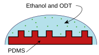
Figure 3 - The PDMS stamp with the ODT is placed on the gold substrate. When the stamp is removed, the ODT in contact with the gold stays stuck to the gold. Thus the pattern from the stamp is transferred to the gold via the ODT
443:
598:
546:
110:
285:
261:
301:
436:
31:
Figure 2 - ODT from the solution settles down onto the PDMS stamp. Stamp now has ODT attached to it which acts as the ink.
53:
100:
486:
536:
471:
141:
81:
of soft lithography expanded rapidly from 1995 to 2005. Soft lithography tools are now commercially available.
429:
78:
511:
481:
476:
23:
Figure 1 - "Inking" a stamp. PDMS stamp with pattern is placed in
Ethanol and ODT (octadecanethiol) solution
551:
105:
313:
242:
95:
526:
359:
330:
253:
64:
556:
516:
158:
74:
59:
using "elastomeric stamps, molds, and conformable photomasks". It is called "soft" because it uses
531:
383:
121:
521:
375:
305:
257:
166:
More pattern-transferring methods than traditional lithography techniques (more "ink" options)
466:
408:
367:
338:
297:
173:
137:
577:
452:
281:
190:
363:
350:
Quake, S. R.; Scherer, A. (2000). "From micro- to nanofabrication with soft materials".
334:
35:
572:
70:
Soft lithography is generally used to construct features measured on the micrometer to
27:
19:
413:
396:
592:
152:
136:
Soft lithography has some unique advantages over other forms of lithography (such as
342:
387:
129:
371:
180:
vs ~100 nm). The resolution depends on the mask used and can reach 6 nm.
90:
45:
302:
10.1002/(SICI)1521-3773(19980316)37:5<550::AID-ANIE550>3.0.CO;2-G
177:
163:
Well-suited for applications involving large or nonplanar (nonflat) surfaces
71:
60:
56:
379:
309:
208:
In the words of Rogers and Nuzzo, p. 50, as cited in "Further reading"
496:
250:
125:
421:
219:"Research Micro Stamps: Commercially available micro stamps on tv"
218:
120:
34:
26:
18:
169:
Does not need a photo-reactive surface to create a nanostructure
425:
148:
Lower cost than traditional photolithography in mass production
321:
Xia, Y.; Whitesides, G. M. (1998). "Soft
Lithography. In".
397:"February). Recent progress in soft lithography. In"
565:
504:
459:
132:deposited by soft lithography with PDMS stamp.
16:Techniques that create structures using stamps
437:
52:is a family of techniques for fabricating or
8:
444:
430:
422:
412:
77:. According to Rogers and Nuzzo (2005),
201:
111:Patterning by etching at the nanoscale
7:
395:Rogers, J. A.; Nuzzo, R. G. (2005).
247:Nanocomputers and Swarm Intelligence
14:
495:
157:Well-suited for applications in
151:Well-suited for applications in
343:10.1146/annurev.matsci.28.1.153
144:). They include the following:
599:Lithography (microfabrication)
1:
414:10.1016/S1369-7021(05)00702-9
372:10.1126/science.290.5496.1536
176:in laboratory settings (~30
101:Multilayer soft lithography
615:
290:Angew. Chem. Int. Ed. Engl
493:
142:electron beam lithography
63:materials, most notably
512:Molecular self-assembly
243:Waldner, Jean-Baptiste
133:
106:Nanosphere lithography
41:
32:
24:
323:Annu. Rev. Mater. Sci
254:John Wiley & Sons
172:Smaller details than
124:
96:Microcontact printing
38:
30:
22:
364:2000Sci...290.1536Q
358:(5496): 1536–1540.
335:1998AnRMS..28..153X
159:plastic electronics
532:Magnetolithography
286:"Soft Lithography"
134:
42:
33:
25:
586:
585:
282:Whitesides, G. M.
263:978-1-84704-002-2
606:
499:
446:
439:
432:
423:
418:
416:
391:
346:
317:
312:. Archived from
268:
267:
239:
233:
232:
230:
229:
215:
209:
206:
174:photolithography
138:photolithography
50:soft lithography
614:
613:
609:
608:
607:
605:
604:
603:
589:
588:
587:
582:
578:Nanoelectronics
561:
500:
491:
455:
453:Nanolithography
450:
401:Materials Today
394:
349:
320:
279:
276:
274:Further reading
271:
264:
241:
240:
236:
227:
225:
217:
216:
212:
207:
203:
199:
191:Nanolithography
187:
119:
87:
17:
12:
11:
5:
612:
610:
602:
601:
591:
590:
584:
583:
581:
580:
575:
573:Nanotechnology
569:
567:
563:
562:
560:
559:
554:
549:
547:Laser printing
544:
539:
534:
529:
524:
519:
514:
508:
506:
502:
501:
494:
492:
490:
489:
487:Scanning probe
484:
479:
474:
469:
463:
461:
457:
456:
451:
449:
448:
441:
434:
426:
420:
419:
392:
347:
318:
316:on 2011-08-12.
296:(5): 551–575.
275:
272:
270:
269:
262:
256:. p. 93.
234:
210:
200:
198:
195:
194:
193:
186:
183:
182:
181:
170:
167:
164:
161:
155:
149:
118:
115:
114:
113:
108:
103:
98:
93:
86:
83:
15:
13:
10:
9:
6:
4:
3:
2:
611:
600:
597:
596:
594:
579:
576:
574:
571:
570:
568:
564:
558:
555:
553:
550:
548:
545:
543:
540:
538:
535:
533:
530:
528:
525:
523:
520:
518:
515:
513:
510:
509:
507:
503:
498:
488:
485:
483:
480:
478:
475:
473:
472:Electron beam
470:
468:
465:
464:
462:
458:
454:
447:
442:
440:
435:
433:
428:
427:
424:
415:
410:
406:
402:
398:
393:
389:
385:
381:
377:
373:
369:
365:
361:
357:
353:
348:
344:
340:
336:
332:
328:
324:
319:
315:
311:
307:
303:
299:
295:
291:
287:
283:
278:
277:
273:
265:
259:
255:
252:
248:
244:
238:
235:
224:
220:
214:
211:
205:
202:
196:
192:
189:
188:
184:
179:
175:
171:
168:
165:
162:
160:
156:
154:
153:biotechnology
150:
147:
146:
145:
143:
139:
131:
127:
123:
116:
112:
109:
107:
104:
102:
99:
97:
94:
92:
89:
88:
84:
82:
80:
76:
73:
68:
66:
62:
58:
55:
51:
47:
37:
29:
21:
541:
407:(2): 50–56.
404:
400:
355:
351:
326:
322:
314:the original
293:
289:
246:
237:
226:. Retrieved
222:
213:
204:
135:
130:streptavidin
69:
49:
43:
557:Proton beam
482:Multiphoton
477:Nanoimprint
329:: 153–184.
79:development
61:elastomeric
54:replicating
552:Nanosphere
249:. London:
228:2017-01-17
197:References
117:Advantages
91:PDMS stamp
57:structures
46:technology
537:Plasmonic
280:Xia, Y.;
128:image of
72:nanometer
593:Category
566:See also
527:Ion beam
380:11090344
310:29711088
284:(1998).
245:(2008).
185:See also
517:Stencil
467:Optical
388:1386132
360:Bibcode
352:Science
331:Bibcode
386:
378:
308:
260:
126:Sarfus
40:"ink."
522:X-ray
505:Other
384:S2CID
85:Types
75:scale
542:Soft
460:Main
376:PMID
306:PMID
258:ISBN
251:ISTE
140:and
65:PDMS
409:doi
368:doi
356:290
339:doi
298:doi
223:RMS
44:In
595::
403:.
399:.
382:.
374:.
366:.
354:.
337:.
327:28
325:.
304:.
294:37
292:.
288:.
221:.
178:nm
67:.
48:,
445:e
438:t
431:v
417:.
411::
405:8
390:.
370::
362::
345:.
341::
333::
300::
266:.
231:.
Text is available under the Creative Commons Attribution-ShareAlike License. Additional terms may apply.