594:, the jitter bound for that hold constraint can be very small, since any variation in that clock signal will affect the two registers equally. For the same example, the jitter bound for the setup constraint must be larger than for the hold constraint, because jitter can vary from clock tick to clock tick. If the source register receives its clock signal from a leaf buffer of the clock distribution network that is far removed from the leaf buffer feeding the destination register, then the jitter bound will have to be larger to account for the different clock paths to the two registers, which may have different noise sources coupling into them.
606:
598:
662:
means that the clock skew between two points varies from cycle to cycle, which is a complexity that is rarely mentioned. Many other authors use the term clock skew only for the spatial variation of clock times, and use the term clock jitter to represent the rest of the total clock timing uncertainty. This of course means that the clock jitter must be different at each component, which again is rarely discussed.
615:
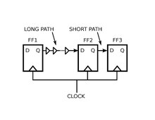
close to having a hold violation: If even a small amount of extra clock delay occurs at FF3, this could destroy the data at the D input of FF3 before the clock arrives to clock it through to FF3's Q output. This could happen even if FF2 and FF3 were physically close to each other, if their clock inputs happened to come from different leaf buffers of a clock distribution network.
167:. Positive skew occurs when the receiving register receives the clock tick later than the transmitting register. Negative skew is the opposite: the transmitting register gets the clock tick later than the receiving register. Zero clock skew refers to the arrival of the clock tick simultaneously at transmitting and receiving register.
636:
problem. In this linear program, zero clock skew is merely a feasible point - the solution to the linear program generally gives a clock period that is less than what is achieved by zero skew. In addition, safety margins greater than or equal to the zero skew case can be guaranteed by setting setup
622:
A common misconception about intentional clock skew is that it is necessarily more dangerous than zero clock skew, or that it requires more precise control of delays in the clock distribution network. However it is the zero skew circuit of Figure 1 that is closer to malfunctioning - a small amount of
175:
There are two types of violation that can be caused by clock skew. One problem is caused when the clock reaches the first register and the clock signal towards the second register travels slower than output of the first register into the second register - the output of the first register reaches the
661:
Thus, in the usual case of sending and receiving registers at different locations, there is no clear way to separate the total clock timing uncertainty into spatial skew and jitter. Thus some authors use the term clock skew to describe the sum of spatial clock skew and clock jitter. This of course
614:
Figures 1 and 2 illustrate a situation where intentional clock skew can benefit a synchronous circuit. In the zero-skew circuit of Figure 1, a long path goes from flip-flop FF1 to flip-flop FF2, and a short path, such as a shift-register path, from FF2 to FF3. The FF2 -> FF3 path is dangerously
609:
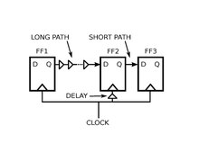
Figure 2. A small amount of delay inserted at the clock input of FF2 guards against a hold violation in the FF2 -> FF3 path, and at the same time allows the FF1 -> FF2 path to operate at a lower clock period. This intentional skew circuit is both safer and faster than the zero skew circuit of
180:
because the previous data is not held long enough at the destination flip-flop to be properly clocked through. Another problem is caused if the destination flip-flop receives the clock tick earlier than the source flip-flop - the data signal has that much less time to reach the destination flip-flop
90:
Ideally, the input to each memory element reaches its final value in time for the next clock tick so that the behavior of the whole circuit can be predicted exactly. The maximum speed at which a system can run must account for the variance that occurs between the various elements of a circuit due to
589:
for the difference in jitter over all source register/destination register pairs. However, if the structure of the clock distribution network is known, different source register/destination register pairs may have different jitter parameters, and a different jitter value may be used for the hold
194:
Where a signal broadly clocks a circuit, the signals/state-transitions it initiates must be stabilized before it signals another set of state transitions -- and that limits the clock's upper frequency. Skew thus decreases the clock frequency at which the circuit will operate correctly. For each
657:
As an approximation, it is often useful to discuss the total clock timing uncertainty between two registers as the sum of spatial clock skew (the spatial differences in clock latency from the clock source), and clock jitter (meaning the non-periodicity of the clock at a particular point in the
185:
occurs, so-called because the new data was not set up and stable before the next clock tick arrived. A hold violation is more serious than a setup violation because it cannot be fixed by increasing the clock period. Positive skew and negative skew cannot negatively impact setup and hold timing
618:
Figure 2 shows how the problem can be fixed with intentional clock skew. A small amount of extra delay is interposed before FF2's clock input, which then safely positions the FF2 -> FF3 path away from its hold violation. As an added benefit, this same extra clock delay relaxes the setup
649:
In addition to clock skew due to static differences in the clock latency from the clock source to each clocked register, no clock signal is perfectly periodic, so that the clock period or clock cycle time varies even at a single component, and this variation is known as clock
156:, material imperfections, and differences in input capacitance on the clock inputs of devices using the clock. As the clock rate of a circuit increases, timing becomes more critical and less variation can be tolerated if the circuit is to function properly.
631:
If the clock arrival times at individual registers are viewed as variables to be adjusted in order to minimize the clock period while satisfying the setup and hold inequalities for all of the paths through the circuit, then the result is a
619:
constraint for the FF1 -> FF2 path. The FF1 -> FF2 path can operate correctly at a clock period that is less than what is required for the zero clock skew case, by an amount equal to the delay of the added clock delay buffer.
283:
365:
665:
Fortunately, in many cases, spatial clock skew remains fairly constant from cycle to cycle, so that the rest of the total clock timing uncertainty can be well approximated by a single common clock jitter value.
640:
Due to the simple form of this linear program, an easily programmed algorithm is available for arriving at a solution. Most CAD systems for VLSI and FPGA design contain facilities for optimizing clock skews.
83:. In a circuit using edge-triggered registers, when the clock edge or tick arrives at a register, the register transfers the register input to the register output, and these new output values flow through
658:
network). Unfortunately, spatial clock skew varies in time from one cycle to the next due to local time-dependent variations in the power supply, local temperature, and noise coupling to other signals.
623:
positive clock skew for the FF2 -> FF3 pair will cause a hold violation, whereas the intentional skew circuit of Figure 2 is more tolerant of unintended delay variations in clock distribution.
75:" that dictates the sequence and pacing of the devices on the circuit. This clock is distributed from a single source to all the memory elements of the circuit, which for example could be
504:
409:
574:
Positive clock skews are good for fixing setup violations, but can cause hold violations. Negative clock skew can guard against a hold violation, but can cause a setup violation.
590:
constraint in contrast to the value for the setup constraint. For example, if the source register and destination register receive their clock signals from a common nearby clock
176:
second register input faster and therefore is clocked replacing the initial data on the second register, or maybe destroying the integrity of the latched data. This is called a
601:
Figure 1. The perils of zero skew. The FF2 -> FF3 path will malfunction with a hold violation if a small amount of extra clock delay to FF3, such as clock jitter, occurs.
473:
94:
In a synchronous circuit, two registers, or flip-flops, are said to be "sequentially adjacent" if a logic path connects them. Given two sequentially adjacent registers R
568:
539:
201:
831:
Tam, S.; Limaye, D.L.; Desai, U.N. (April 2004). "Clock
Generation and Distribution for the 130-nm Itanium 2 Processor with 6-MB On-Die L3 Cache".
289:
152:
Clock skew can be caused by many different things, such as wire-interconnect length, temperature variations, variation in intermediate devices,
778:
767:
833:
57:
975:
654:. At a particular point in a clock distribution network, jitter is the only contributor to the clock timing uncertainty.
195:
source register and destination register connected by a path, the following setup and hold inequalities must be obeyed:
480:
385:
61:
786:
80:
795:
586:
698:) have been designed to reduce clock skew, and produce more stable functions. Some applications (such as
980:
695:
901:
711:
53:
702:) may also use their own synchronization mechanism to avoid reliability problems due to clock skew.
432:
153:
84:
41:
38:
813:
800:
850:
633:
763:
605:
76:
694:
which are comparable across hosts can be affected by clock skew. A number of protocols (e.g.
943:
916:
842:
805:
683:
64:. The instantaneous difference between the readings of any two clocks is called their skew.
546:
517:
68:
874:, 1993 IEEE International Symposium on Circuits and Systems (pp. 1475-1478). IEEE, 1993.
710:
Clock skew is the reason why at fast speeds or long distances, serial interfaces (e.g.
591:
969:
756:
687:
106:
with clock arrival times at the source and destination register clock pins equal to T
854:
597:
690:
with time) of different clocks within the network. Network operations that require
72:
49:
731:
699:
278:{\displaystyle T\geq {\text{reg}}+{\text{path}}_{\text{max}}+J+S-(s_{d}-s_{s})}
936:"Network Time Protocol (Version 3) Specification, Implementation and Analysis"
424:
846:
360:{\displaystyle (s_{d}-s_{s})\leq {\text{reg}}+{\text{path}}_{\text{min}}-J-H}
691:
17:
741:
675:
45:
779:"Clock Distribution Networks in Synchronous Digital Integrated Circuits"
475:
represents the clock skew from the source to the destination registers,
935:
948:
920:
809:
736:
651:
637:
and hold times and jitter bound appropriately in the linear program.
582:
91:
differences in physical composition, temperature, and path length.
604:
596:
87:
to provide the values at register inputs for the next clock tick.
719:
506:
is the path with the shortest delay from source to destination,
715:
411:
is the path with the longest delay from source to destination,
882:
880:
67:
The operation of most digital circuits is synchronized by a
758:
718:) are preferred over parallel interfaces (e.g. parallel
888:
Timing
Analysis and Optimization of Sequential Circuits
872:
Clock distribution design in VLSI circuits-an overview
549:
520:
483:
435:
388:
292:
204:
181:
before the next clock tick. If it fails to do so, a
56:
at different times due to gate or, in more advanced
186:constraints respectively (see inequalities below).
755:
562:
541:is the clock skew to the destination register, and
533:
498:
467:
403:
359:
277:
577:In the above inequalities, a single parameter,
380:reg is the source register's clock to Q delay,
27:Misaligned timing signals from different paths
645:Confusion between clock skew and clock jitter
512:is the hold time of the destination register,
8:
120:respectively, clock skew can be defined as:
499:{\displaystyle {\text{path}}_{\text{min}}}
404:{\displaystyle {\text{path}}_{\text{max}}}
947:
799:
570:is the clock skew to the source register.
554:
548:
525:
519:
490:
485:
482:
456:
443:
434:
395:
390:
387:
339:
334:
325:
313:
300:
291:
266:
253:
225:
220:
211:
203:
863:
682:describes the difference in frequency (
886:Maheshwari, N., and Sapatnekar, S.S.,
7:
834:IEEE Journal of Solid-State Circuits
159:There are two types of clock skew:
48:systems) in which the same sourced
25:
909:IEEE Transactions on Computers
462:
436:
319:
293:
272:
246:
1:
777:Friedman, Eby G. (May 2001).
585:. This parameter must be an
468:{\displaystyle (s_{d}-s_{s})}
900:Fishburn, J.P. (July 1990).
417:is an upper bound on jitter,
427:of the destination register
997:
902:"Clock skew optimization"
754:Friedman, Eby G. (1995).
674:On a network such as the
581:, is used to account for
847:10.1109/JSSC.2004.825121
62:signal propagation delay
58:semiconductor technology
787:Proceedings of the IEEE
42:digital circuit systems
611:
602:
564:
535:
500:
469:
405:
361:
279:
976:Electrical parameters
696:Network Time Protocol
608:
600:
565:
563:{\displaystyle s_{s}}
536:
534:{\displaystyle s_{d}}
501:
470:
406:
362:
280:
52:arrives at different
37:) is a phenomenon in
712:Serial Attached SCSI
547:
518:
481:
433:
386:
377:is the clock period,
290:
202:
154:capacitive coupling
85:combinational logic
934:Mills, D. (1992).
634:Linear Programming
612:
603:
560:
531:
496:
465:
401:
357:
275:
33:(sometimes called
769:978-0-7803-1058-2
493:
488:
398:
393:
342:
337:
328:
228:
223:
214:
148:In circuit design
16:(Redirected from
988:
960:
959:
957:
956:
951:
949:10.17487/RFC1305
931:
925:
924:
921:10.1109/12.55696
906:
897:
891:
884:
875:
870:Friedman, E. G.
868:
858:
827:
825:
824:
818:
812:. Archived from
810:10.1109/5.929649
803:
783:
773:
761:
684:first derivative
569:
567:
566:
561:
559:
558:
540:
538:
537:
532:
530:
529:
505:
503:
502:
497:
495:
494:
491:
489:
486:
474:
472:
471:
466:
461:
460:
448:
447:
410:
408:
407:
402:
400:
399:
396:
394:
391:
366:
364:
363:
358:
344:
343:
340:
338:
335:
329:
326:
318:
317:
305:
304:
284:
282:
281:
276:
271:
270:
258:
257:
230:
229:
226:
224:
221:
215:
212:
143:
21:
996:
995:
991:
990:
989:
987:
986:
985:
966:
965:
964:
963:
954:
952:
933:
932:
928:
904:
899:
898:
894:
890:, Kluwer, 1999.
885:
878:
869:
865:
830:
822:
820:
816:
781:
776:
770:
753:
750:
728:
708:
672:
647:
629:
550:
545:
544:
521:
516:
515:
484:
479:
478:
452:
439:
431:
430:
389:
384:
383:
333:
309:
296:
288:
287:
262:
249:
219:
200:
199:
192:
190:Beneficial skew
183:setup violation
173:
150:
142:
135:
128:
121:
119:
112:
105:
99:
69:periodic signal
28:
23:
22:
15:
12:
11:
5:
994:
992:
984:
983:
978:
968:
967:
962:
961:
940:tools.ietf.org
926:
915:(7): 945–951.
892:
876:
862:
861:
860:
859:
828:
794:(5): 665–692.
774:
768:
762:. IEEE Press.
749:
746:
745:
744:
739:
734:
727:
724:
707:
704:
671:
668:
646:
643:
628:
625:
572:
571:
557:
553:
542:
528:
524:
513:
507:
476:
464:
459:
455:
451:
446:
442:
438:
428:
418:
412:
381:
378:
368:
367:
356:
353:
350:
347:
332:
324:
321:
316:
312:
308:
303:
299:
295:
285:
274:
269:
265:
261:
256:
252:
248:
245:
242:
239:
236:
233:
218:
210:
207:
191:
188:
178:hold violation
172:
169:
149:
146:
137:
130:
123:
114:
107:
101:
95:
26:
24:
14:
13:
10:
9:
6:
4:
3:
2:
993:
982:
979:
977:
974:
973:
971:
950:
945:
941:
937:
930:
927:
922:
918:
914:
910:
903:
896:
893:
889:
883:
881:
877:
873:
867:
864:
856:
852:
848:
844:
840:
836:
835:
829:
819:on 2015-06-01
815:
811:
807:
802:
801:10.1.1.7.7824
797:
793:
789:
788:
780:
775:
771:
765:
760:
759:
752:
751:
747:
743:
740:
738:
735:
733:
730:
729:
725:
723:
721:
717:
713:
705:
703:
701:
697:
693:
689:
685:
681:
677:
669:
667:
663:
659:
655:
653:
644:
642:
638:
635:
626:
624:
620:
616:
607:
599:
595:
593:
588:
584:
580:
575:
555:
551:
543:
526:
522:
514:
511:
508:
477:
457:
453:
449:
444:
440:
429:
426:
422:
419:
416:
413:
382:
379:
376:
373:
372:
371:
354:
351:
348:
345:
330:
322:
314:
310:
306:
301:
297:
286:
267:
263:
259:
254:
250:
243:
240:
237:
234:
231:
216:
208:
205:
198:
197:
196:
189:
187:
184:
179:
170:
168:
166:
165:positive skew
162:
161:negative skew
157:
155:
147:
145:
141:
134:
127:
118:
111:
104:
98:
92:
88:
86:
82:
78:
74:
70:
65:
63:
59:
55:
51:
47:
43:
40:
36:
32:
19:
981:Clock signal
953:. Retrieved
939:
929:
912:
908:
895:
887:
871:
866:
838:
832:
821:. Retrieved
814:the original
791:
785:
757:
709:
700:game servers
679:
673:
670:On a network
664:
660:
656:
648:
639:
630:
627:Optimal skew
621:
617:
613:
578:
576:
573:
509:
420:
414:
374:
369:
193:
182:
177:
174:
171:Harmful skew
164:
160:
158:
151:
139:
132:
125:
116:
109:
102:
96:
93:
89:
71:known as a "
66:
50:clock signal
34:
30:
29:
732:Clock drift
587:upper bound
39:synchronous
35:timing skew
18:Timing skew
970:Categories
955:2017-10-30
823:2017-01-09
748:References
706:Interfaces
692:timestamps
680:clock skew
425:setup time
81:flip-flops
54:components
31:Clock skew
796:CiteSeerX
610:Figure 1.
450:−
352:−
346:−
323:≤
307:−
260:−
244:−
209:≥
77:registers
44:(such as
855:31388328
742:Skewness
726:See also
676:internet
46:computer
423:is the
60:, wire
853:
798:
766:
737:Jitter
688:offset
652:jitter
592:buffer
583:jitter
370:where
905:(PDF)
851:S2CID
841:(4).
817:(PDF)
782:(PDF)
124:skew
113:and T
100:and R
73:clock
764:ISBN
720:SCSI
487:path
392:path
336:path
222:path
163:and
126:i, j
944:doi
917:doi
843:doi
806:doi
722:).
716:USB
714:or
686:of
492:min
397:max
341:min
327:reg
227:max
213:reg
136:− T
129:= T
79:or
972::
942:.
938:.
913:39
911:.
907:.
879:^
849:.
839:39
837:.
804:.
792:89
790:.
784:.
678:,
144:.
958:.
946::
923:.
919::
857:.
845::
826:.
808::
772:.
579:J
556:s
552:s
527:d
523:s
510:H
463:)
458:s
454:s
445:d
441:s
437:(
421:S
415:J
375:T
355:H
349:J
331:+
320:)
315:s
311:s
302:d
298:s
294:(
273:)
268:s
264:s
255:d
251:s
247:(
241:S
238:+
235:J
232:+
217:+
206:T
140:j
138:C
133:i
131:C
122:T
117:j
115:C
110:i
108:C
103:j
97:i
20:)
Text is available under the Creative Commons Attribution-ShareAlike License. Additional terms may apply.