113:
specifically when recording absorbance readings from
Ultraviolet-visible Spectroscopy, since thicker films have lower optical transmittance and typically do not allow light to shine through in comparison to thinner films allowing light to go through before the optical density of the film becomes too low. Additionally, films with lower absorbance quality are not as ideal of candidates for processes such as Cyclic Voltammetry because the low absorbance hinders electrochemical tuning of cations when in an electrochemical cell. Thinner films in this regard have more desirable optical properties that can be tuned for energy storage technologies because of their spin coated influenced properties. However, spin coating thicker films of
520:
28:
85:
of the solution, and the solvent. Pioneering theoretical analysis of spin coating was undertaken by Emslie et al., and has been extended by many subsequent authors (including Wilson et al., who studied the rate of spreading in spin coating; and
Danglad-Flores et al., who found a universal description
112:
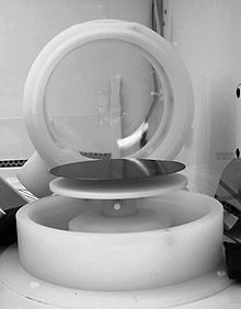
One advantage to spin coating thin films is the uniformity of the film thickness. Owing to self-leveling, thicknesses do not vary more than 1%. The thickness of films produced in this manner may also affect the optical properties of such materials. This is important for electrochemical testing,
50:. Usually a small amount of coating material in liquid form is applied on the center of the substrate, which is either spinning at low speed or not spinning at all. The substrate is then rotated at speeds up to 10,000 rpm to spread the coating material by
109:
thick. Photoresist is typically spun at 20 to 80 revolutions per second for 30 to 60 seconds. It is also widely used for the fabrication of planar photonic structures made of polymers.
65:
Rotation is continued while the fluid spins off the edges of the substrate, until the desired thickness of the film is achieved. The applied solvent is usually
457:
Schubert, Dirk W.; Dunkel, Thomas (2003). "Spin coating from a molecular point of view: its concentration regimes, influence of molar mass and distribution".
327:
Hanaor, D.A.H.; Triani, G.; Sorrell, C.C. (2011). "Morphology and photocatalytic activity of highly oriented mixed phase titanium dioxide thin films".
585:
561:
155:
453:
S. Middleman and A.K. Hochberg. "Process
Engineering Analysis in Semiconductor Device Fabrication". McGraw-Hill, p. 313 (1993)
590:
580:
500:
554:
97:
precursors, where it can be used to create uniform thin films with nanoscale thicknesses. It is used intensively in
595:
547:
66:
505:
250:
215:
47:
527:
402:
482:
432:
362:
336:
266:
206:
Emslie, A. G.; Bonner, F. T.; Peck, L. G. (1958). "Flow of a viscous liquid on a rotating disk".
147:
474:
354:
188:
151:
51:
466:
422:
414:
346:
307:
297:
258:
223:
180:
143:
98:
90:
403:"The limits of edge bead planarization and surface levelling in spin-coated liquid films"
380:
254:
219:
531:
241:
Wilson, S. K.; Hunt, R.; Duffy, B. R. (2000). "The rate of spreading in spin coating".
574:
436:
312:
82:
74:
486:
366:
270:
350:
171:
Scriven, L. E. (1988). "Physics and
Applications of DIP Coating and Spin Coating".
121:
can result in relatively large edge beads whose planarization has physical limits.
77:
of spinning, the thinner the film. The thickness of the film also depends on the
118:
102:
70:
32:
418:
470:
427:
302:
285:
262:
106:
478:
358:
192:
78:
43:
17:
184:
114:
94:
93:
of functional oxide layers on glass or single crystal substrates using
286:"Deposition of polymer films by spin casting: A quantitative analysis"
227:
506:
Deposition of polymer films by spin casting: A quantitative analysis
519:
27:
341:
26:
138:
Cohen, Edward; Lightfoot, E. J. (2011). "Coating
Processes".
284:
Danglad-Flores, J.; Eickelmann, S.; Riegler, H. (2018).
535:
31:
501:Spin Coating of Thin and Ultrathin Polymer Films
140:Kirk-Othmer Encyclopedia of Chemical Technology
407:Journal of Micromechanics and Microengineering
54:. A machine used for spin coating is called a
555:
8:
148:10.1002/0471238961.1921182203150805.a01.pub3
562:
548:
86:to predict the deposited film thickness).
426:
340:
311:
301:
179:. Cambridge University Press (CUP): 717.
130:
42:is a procedure used to deposit uniform
7:
516:
514:
465:(5). Informa UK Limited: 314–321.
35:to the surface of a silicon wafer.
25:
586:Semiconductor device fabrication
518:
329:Surface and Coatings Technology
89:Spin coating is widely used in
459:Materials Research Innovations
351:10.1016/j.surfcoat.2011.01.007
335:(12). Elsevier BV: 3658–3664.
1:
534:. You can help Knowledge by
612:
513:
383:. Inseto. November 4, 2020
471:10.1007/s10019-003-0270-2
313:21.11116/0000-0000-2D6C-6
303:10.1016/j.ces.2018.01.012
263:10.1017/S0022112000008089
419:10.1088/1361-6439/ab60be
142:. New York: John Wiley.
401:Arscott, Steve (2020).
381:"What Is Spin Coating?"
101:, to deposit layers of
530:-related article is a
36:
69:, and simultaneously
30:
591:Thin film deposition
581:Industrial processes
185:10.1557/proc-121-717
255:2000JFM...413...65W
220:1958JAP....29..858E
428:20.500.12210/44092
37:
543:
542:
228:10.1063/1.1723300
73:. The higher the
52:centrifugal force
16:(Redirected from
603:
564:
557:
550:
522:
515:
490:
441:
440:
430:
398:
392:
391:
389:
388:
377:
371:
370:
344:
324:
318:
317:
315:
305:
281:
275:
274:
238:
232:
231:
203:
197:
196:
168:
162:
161:
135:
99:photolithography
91:microfabrication
21:
611:
610:
606:
605:
604:
602:
601:
600:
571:
570:
569:
568:
511:
497:
456:
450:
448:Further reading
445:
444:
400:
399:
395:
386:
384:
379:
378:
374:
326:
325:
321:
283:
282:
278:
240:
239:
235:
205:
204:
200:
173:MRS Proceedings
170:
169:
165:
158:
137:
136:
132:
127:
23:
22:
15:
12:
11:
5:
609:
607:
599:
598:
596:Industry stubs
593:
588:
583:
573:
572:
567:
566:
559:
552:
544:
541:
540:
523:
509:
508:
503:
496:
495:External links
493:
492:
491:
454:
449:
446:
443:
442:
393:
372:
319:
290:Chem. Eng. Sci
276:
233:
214:(5): 858–862.
198:
163:
157:978-0471238966
156:
129:
128:
126:
123:
24:
14:
13:
10:
9:
6:
4:
3:
2:
608:
597:
594:
592:
589:
587:
584:
582:
579:
578:
576:
565:
560:
558:
553:
551:
546:
545:
539:
537:
533:
529:
524:
521:
517:
512:
507:
504:
502:
499:
498:
494:
488:
484:
480:
476:
472:
468:
464:
460:
455:
452:
451:
447:
438:
434:
429:
424:
420:
416:
413:(2): 025003.
412:
408:
404:
397:
394:
382:
376:
373:
368:
364:
360:
356:
352:
348:
343:
338:
334:
330:
323:
320:
314:
309:
304:
299:
295:
291:
287:
280:
277:
272:
268:
264:
260:
256:
252:
248:
244:
243:J. Fluid Mech
237:
234:
229:
225:
221:
217:
213:
209:
208:J. Appl. Phys
202:
199:
194:
190:
186:
182:
178:
174:
167:
164:
159:
153:
149:
145:
141:
134:
131:
124:
122:
120:
116:
110:
108:
104:
100:
96:
92:
87:
84:
83:concentration
80:
76:
75:angular speed
72:
68:
63:
61:
57:
53:
49:
45:
41:
34:
29:
19:
536:expanding it
525:
510:
462:
458:
410:
406:
396:
385:. Retrieved
375:
332:
328:
322:
293:
289:
279:
249:(1): 65–88.
246:
242:
236:
211:
207:
201:
176:
172:
166:
139:
133:
119:photoresists
111:
88:
64:
59:
58:, or simply
55:
40:Spin coating
39:
38:
296:: 257–264.
103:photoresist
56:spin coater
33:photoresist
18:Spin coated
575:Categories
387:2023-05-24
125:References
107:micrometre
71:evaporates
48:substrates
46:onto flat
44:thin films
479:1432-8917
437:214580612
359:0257-8972
342:1303.2741
193:1946-4274
79:viscosity
528:industry
487:98374776
367:96130259
271:14585243
115:polymers
105:about 1
67:volatile
251:Bibcode
216:Bibcode
95:sol-gel
60:spinner
485:
477:
435:
365:
357:
269:
191:
154:
526:This
483:S2CID
433:S2CID
363:S2CID
337:arXiv
267:S2CID
532:stub
475:ISSN
355:ISSN
189:ISSN
152:ISBN
117:and
81:and
467:doi
423:hdl
415:doi
347:doi
333:205
308:hdl
298:doi
294:179
259:doi
247:413
224:doi
181:doi
177:121
144:doi
577::
481:.
473:.
461:.
431:.
421:.
411:30
409:.
405:.
361:.
353:.
345:.
331:.
306:.
292:.
288:.
265:.
257:.
245:.
222:.
212:29
210:.
187:.
175:.
150:.
62:.
563:e
556:t
549:v
538:.
489:.
469::
463:7
439:.
425::
417::
390:.
369:.
349::
339::
316:.
310::
300::
273:.
261::
253::
230:.
226::
218::
195:.
183::
160:.
146::
20:)
Text is available under the Creative Commons Attribution-ShareAlike License. Additional terms may apply.